- 您现在的位置:买卖IC网 > PDF目录80533 > MPC8560CPX667JC (FREESCALE SEMICONDUCTOR INC) 32-BIT, 667 MHz, RISC PROCESSOR, PBGA783 PDF资料下载
参数资料
| 型号: | MPC8560CPX667JC |
| 厂商: | FREESCALE SEMICONDUCTOR INC |
| 元件分类: | 微控制器/微处理器 |
| 英文描述: | 32-BIT, 667 MHz, RISC PROCESSOR, PBGA783 |
| 封装: | 29 X 29 MM, 3.75 MM HEIGHT, 1 MM PITCH, PLASTIC, FCBGA-783 |
| 文件页数: | 12/104页 |
| 文件大小: | 1244K |
| 代理商: | MPC8560CPX667JC |
第1页第2页第3页第4页第5页第6页第7页第8页第9页第10页第11页当前第12页第13页第14页第15页第16页第17页第18页第19页第20页第21页第22页第23页第24页第25页第26页第27页第28页第29页第30页第31页第32页第33页第34页第35页第36页第37页第38页第39页第40页第41页第42页第43页第44页第45页第46页第47页第48页第49页第50页第51页第52页第53页第54页第55页第56页第57页第58页第59页第60页第61页第62页第63页第64页第65页第66页第67页第68页第69页第70页第71页第72页第73页第74页第75页第76页第77页第78页第79页第80页第81页第82页第83页第84页第85页第86页第87页第88页第89页第90页第91页第92页第93页第94页第95页第96页第97页第98页第99页第100页第101页第102页第103页第104页
MPC8560 Integrated Processor Hardware Specifications, Rev. 5
Freescale Semiconductor
15
Clock Timing
4
Clock Timing
4.1
System Clock Timing
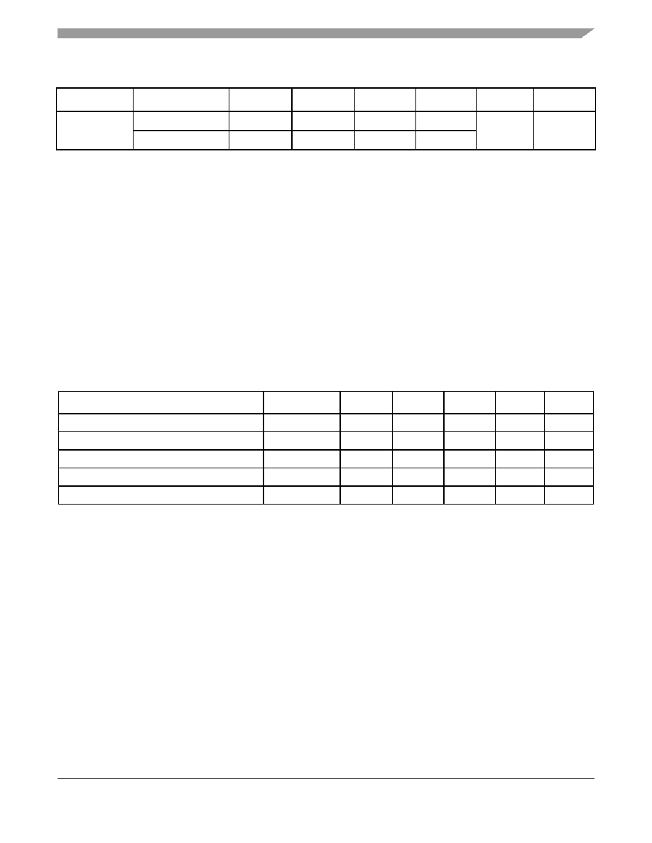
Table 7 provides the system clock (SYSCLK) AC timing specifications for the MPC8560.
TDMA or TDMB
Nibble mode
—
10
—
mW
7
Per channel
—
5
—
Notes:
1. GVDD=2.5, ECC enabled, 66% bus utilization, 33% write cycles, 10pF load on data, 10pF load on address/command, 10pF
load on clock
2. OVDD=3.3, 30pF load per pin, 54% bus utilization, 33% write cycles
3. OVDD=3.3, 25pF load per pin, 5pF load on clock, 40% bus utilization, 33% write cycles
4. VDD=1.2, OVDD=3.3
5. LVDD=2.5/3.3, 15pF load per pin, 25% bus utilization
6. Power dissipation for one TSEC only
7. OVDD=3.3, 10pF load per pin, 50% bus utilization
Table 7. SYSCLK AC Timing Specifications
Parameter/Condition
Symbol
Min
Typical
Max
Unit
Notes
SYSCLK frequency
fSYSCLK
—
166
MHz
1
SYSCLK cycle time
tSYSCLK
6.0
—
ns
—
SYSCLK rise and fall time
tKH, tKL
0.6
1.0
1.2
ns
2
SYSCLK duty cycle
tKHKL/tSYSCLK
40
—
60
%
3
SYSCLK jitter
—
+/- 150
ps
4, 5
Notes:
1. Caution: The CCB to SYSCLK ratio and e500 core to CCB ratio settings must be chosen such that the resulting SYSCLK
frequency, e500 (core) frequency, and CCB frequency do not exceed their respective maximum or minimum operating
frequencies. Refer to Section 15.2, “Platform/System PLL Ratio,” and Section 15.3, “e500 Core PLL Ratio,” for ratio settings.
2. Rise and fall times for SYSCLK are measured at 0.6 V and 2.7 V.
3. Timing is guaranteed by design and characterization.
4. This represents the total input jitter—short term and long term—and is guaranteed by design.
5. For spread spectrum clocking, guidelines are +/-1% of the input frequency with a maximum of 60 kHz of modulation
regardless of the input frequency.
Table 6. Estimated Typical I/O Power Consumption (continued)
Interface
Parameter
GVDD (2.5 V) OVDD (3.3 V) LVDD (3.3 V) LVDD (2.5 V)
Units
Notes
相关PDF资料 |
PDF描述 |
|---|---|
| M901-01I669.3266LF | 669.3266 MHz, OTHER CLOCK GENERATOR, CQCC36 |
| M906-01-125.2500LF | 125 MHz, OTHER CLOCK GENERATOR, CQCC36 |
| M906-01-156.2500LF | 156.25 MHz, OTHER CLOCK GENERATOR, CQCC36 |
| M908-01I187.5000LF | 187.5 MHz, OTHER CLOCK GENERATOR, CQCC36 |
| M908-02-175.0000 | 175 MHz, OTHER CLOCK GENERATOR, CQCC36 |
相关代理商/技术参数 |
参数描述 |
|---|---|
| MPC8560CPX667LB | 功能描述:微处理器 - MPU PQ 3 8560-DRACOM RoHS:否 制造商:Atmel 处理器系列:SAMA5D31 核心:ARM Cortex A5 数据总线宽度:32 bit 最大时钟频率:536 MHz 程序存储器大小:32 KB 数据 RAM 大小:128 KB 接口类型:CAN, Ethernet, LIN, SPI,TWI, UART, USB 工作电源电压:1.8 V to 3.3 V 最大工作温度:+ 85 C 安装风格:SMD/SMT 封装 / 箱体:FBGA-324 |
| MPC8560CVT667JB | 功能描述:微处理器 - MPU PQ 3 8560-DRACOM RoHS:否 制造商:Atmel 处理器系列:SAMA5D31 核心:ARM Cortex A5 数据总线宽度:32 bit 最大时钟频率:536 MHz 程序存储器大小:32 KB 数据 RAM 大小:128 KB 接口类型:CAN, Ethernet, LIN, SPI,TWI, UART, USB 工作电源电压:1.8 V to 3.3 V 最大工作温度:+ 85 C 安装风格:SMD/SMT 封装 / 箱体:FBGA-324 |
| MPC8560CVT667JC | 功能描述:微处理器 - MPU PQ 3 8560-DRACOM RoHS:否 制造商:Atmel 处理器系列:SAMA5D31 核心:ARM Cortex A5 数据总线宽度:32 bit 最大时钟频率:536 MHz 程序存储器大小:32 KB 数据 RAM 大小:128 KB 接口类型:CAN, Ethernet, LIN, SPI,TWI, UART, USB 工作电源电压:1.8 V to 3.3 V 最大工作温度:+ 85 C 安装风格:SMD/SMT 封装 / 箱体:FBGA-324 |
| MPC8560CVT667LB | 功能描述:微处理器 - MPU PQ 3 8560 Dracom RoHS:否 制造商:Atmel 处理器系列:SAMA5D31 核心:ARM Cortex A5 数据总线宽度:32 bit 最大时钟频率:536 MHz 程序存储器大小:32 KB 数据 RAM 大小:128 KB 接口类型:CAN, Ethernet, LIN, SPI,TWI, UART, USB 工作电源电压:1.8 V to 3.3 V 最大工作温度:+ 85 C 安装风格:SMD/SMT 封装 / 箱体:FBGA-324 |
| MPC8560PX667LB | 功能描述:微处理器 - MPU PQ 3 8560-DRACOM RoHS:否 制造商:Atmel 处理器系列:SAMA5D31 核心:ARM Cortex A5 数据总线宽度:32 bit 最大时钟频率:536 MHz 程序存储器大小:32 KB 数据 RAM 大小:128 KB 接口类型:CAN, Ethernet, LIN, SPI,TWI, UART, USB 工作电源电压:1.8 V to 3.3 V 最大工作温度:+ 85 C 安装风格:SMD/SMT 封装 / 箱体:FBGA-324 |
发布紧急采购,3分钟左右您将得到回复。