- 您现在的位置:买卖IC网 > PDF目录4041 > MPC8568EVTAUJJ (Freescale Semiconductor)MPU POWERQUICC III 1023-PBGA PDF资料下载
参数资料
| 型号: | MPC8568EVTAUJJ |
| 厂商: | Freescale Semiconductor |
| 文件页数: | 109/139页 |
| 文件大小: | 0K |
| 描述: | MPU POWERQUICC III 1023-PBGA |
| 标准包装: | 24 |
| 系列: | MPC85xx |
| 处理器类型: | 32-位 MPC85xx PowerQUICC III |
| 速度: | 1.333GHz |
| 电压: | 1.1V |
| 安装类型: | 表面贴装 |
| 封装/外壳: | 1023-BBGA,FCBGA |
| 供应商设备封装: | 1023-FCPBGA(33x33) |
| 包装: | 托盘 |
第1页第2页第3页第4页第5页第6页第7页第8页第9页第10页第11页第12页第13页第14页第15页第16页第17页第18页第19页第20页第21页第22页第23页第24页第25页第26页第27页第28页第29页第30页第31页第32页第33页第34页第35页第36页第37页第38页第39页第40页第41页第42页第43页第44页第45页第46页第47页第48页第49页第50页第51页第52页第53页第54页第55页第56页第57页第58页第59页第60页第61页第62页第63页第64页第65页第66页第67页第68页第69页第70页第71页第72页第73页第74页第75页第76页第77页第78页第79页第80页第81页第82页第83页第84页第85页第86页第87页第88页第89页第90页第91页第92页第93页第94页第95页第96页第97页第98页第99页第100页第101页第102页第103页第104页第105页第106页第107页第108页当前第109页第110页第111页第112页第113页第114页第115页第116页第117页第118页第119页第120页第121页第122页第123页第124页第125页第126页第127页第128页第129页第130页第131页第132页第133页第134页第135页第136页第137页第138页第139页
MPC8568E/MPC8567E PowerQUICC III Integrated Processor Hardware Specifications, Rev. 1
Freescale Semiconductor
71
PCI Express
14.3
Clocking Dependencies
The ports on the two ends of a link must transmit data at a rate that is within 600 parts per million (ppm)
of each other at all times. This is specified to allow bit rate clock sources with a +/– 300 ppm tolerance.
14.4
Physical Layer Specifications
The following is a summary of the specifications for the physical layer of PCI Express on this device. For
further details as well as the specifications of the Transport and Data Link layer please use the PCI
EXPRESS Base Specification. REV. 1.0a document.
14.4.1
Differential Transmitter (TX) Output
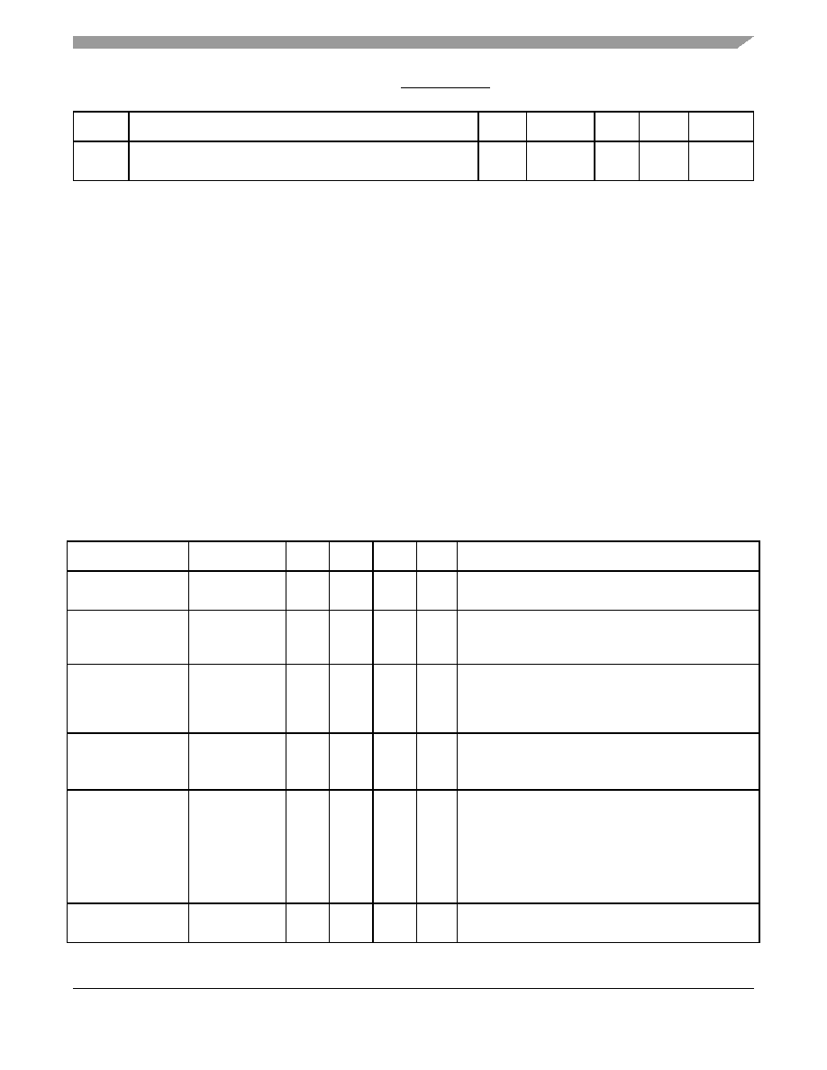
Table 51 defines the specifications for the differential output at all transmitters (TXs). The parameters are
specified at the component pins.
tREFPJ
Phase jitter. Deviation in edge location with respect to mean
edge location
–50
—
50
ps
—
Notes:
1. Typical based on PCI Express Specification 2.0.
Table 51. Differential Transmitter (TX) Output Specifications
Symbol
Parameter
Min
Nom
Max
Units
Comments
UI
Unit Interval
399.88
400
400.12
ps
Each UI is 400 ps ± 300 ppm. UI does not account for
Spread Spectrum Clock dictated variations. See Note 1.
VTX-DIFFp-p
Differential
Peak-to-Peak
Output Voltage
0.8
—
1.2
V
VTX-DIFFp-p = 2*|VTX-D+ – VTX-D-| See Note 2.
VTX-DE-RATIO
De- Emphasized
Differential
Output Voltage
(Ratio)
–3.0
–3.5
–4.0
dB
Ratio of the VTX-DIFFp-p of the second and following bits
after a transition divided by the VTX-DIFFp-p of the first bit
after a transition. See Note 2.
TTX-EYE
Minimum TX Eye
Width
0.70
—
UI
The maximum Transmitter jitter can be derived as
TTX-MAX-JITTER = 1 – TTX-EYE= 0.3 UI.
See Notes 2 and 3.
TTX-EYE-MEDIAN-to-
MAX-JITTER
Maximum time
between the jitter
median and
maximum
deviation from
the median.
—
0.15
UI
Jitter is defined as the measurement variation of the
crossing points (VTX-DIFFp-p = 0 V) in relation to a
recovered TX UI. A recovered TX UI is calculated over
3500 consecutive unit intervals of sample data. Jitter is
measured using all edges of the 250 consecutive UI in
the center of the 3500 UI used for calculating the TX UI.
See Notes 2 and 3.
TTX-RISE, TTX-FALL
D+/D- TX Output
Rise/Fall Time
0.125
—
UI
See Notes 2 and 5
Table 50. SD_REF_CLK and SD_REF_CLK AC Requirements
Symbol
Parameter Description
Min
Typical
Max
Units
Notes
相关PDF资料 |
PDF描述 |
|---|---|
| MPC8572VTATLE | MPU POWERQUICC III 1023FCPBGA |
| MPC8572EVTARLE | MPU POWERQUICC III 1023FCPBGA |
| MPC8572VTATLD | MPU POWERQUICC III 1023-PBGA |
| IDT70V9089S15PF8 | IC SRAM 512KBIT 15NS 100TQFP |
| MPC8572EPXARLD | MPU POWERQUICC III 1023-PBGA |
相关代理商/技术参数 |
参数描述 |
|---|---|
| MPC8568VTAQGG | 功能描述:微处理器 - MPU 8568 1GHz Non Encrypt RoHS:否 制造商:Atmel 处理器系列:SAMA5D31 核心:ARM Cortex A5 数据总线宽度:32 bit 最大时钟频率:536 MHz 程序存储器大小:32 KB 数据 RAM 大小:128 KB 接口类型:CAN, Ethernet, LIN, SPI,TWI, UART, USB 工作电源电压:1.8 V to 3.3 V 最大工作温度:+ 85 C 安装风格:SMD/SMT 封装 / 箱体:FBGA-324 |
| MPC8568VTAUJJ | 功能描述:微处理器 - MPU 8568 1.33GHz Non Encrypt RoHS:否 制造商:Atmel 处理器系列:SAMA5D31 核心:ARM Cortex A5 数据总线宽度:32 bit 最大时钟频率:536 MHz 程序存储器大小:32 KB 数据 RAM 大小:128 KB 接口类型:CAN, Ethernet, LIN, SPI,TWI, UART, USB 工作电源电压:1.8 V to 3.3 V 最大工作温度:+ 85 C 安装风格:SMD/SMT 封装 / 箱体:FBGA-324 |
| MPC8569CVTANKGB | 功能描述:数字信号处理器和控制器 - DSP, DSC 8569 XT 800/600/400 r2.1 RoHS:否 制造商:Microchip Technology 核心:dsPIC 数据总线宽度:16 bit 程序存储器大小:16 KB 数据 RAM 大小:2 KB 最大时钟频率:40 MHz 可编程输入/输出端数量:35 定时器数量:3 设备每秒兆指令数:50 MIPs 工作电源电压:3.3 V 最大工作温度:+ 85 C 封装 / 箱体:TQFP-44 安装风格:SMD/SMT |
| MPC8569CVTAQLJB | 功能描述:数字信号处理器和控制器 - DSP, DSC 8569 XT 1067/667/533 r2.1 RoHS:否 制造商:Microchip Technology 核心:dsPIC 数据总线宽度:16 bit 程序存储器大小:16 KB 数据 RAM 大小:2 KB 最大时钟频率:40 MHz 可编程输入/输出端数量:35 定时器数量:3 设备每秒兆指令数:50 MIPs 工作电源电压:3.3 V 最大工作温度:+ 85 C 封装 / 箱体:TQFP-44 安装风格:SMD/SMT |
| MPC8569ECVTANKGB | 功能描述:数字信号处理器和控制器 - DSP, DSC 8569E XT 800/600/400 r2.1 RoHS:否 制造商:Microchip Technology 核心:dsPIC 数据总线宽度:16 bit 程序存储器大小:16 KB 数据 RAM 大小:2 KB 最大时钟频率:40 MHz 可编程输入/输出端数量:35 定时器数量:3 设备每秒兆指令数:50 MIPs 工作电源电压:3.3 V 最大工作温度:+ 85 C 封装 / 箱体:TQFP-44 安装风格:SMD/SMT |
发布紧急采购,3分钟左右您将得到回复。