- 您现在的位置:买卖IC网 > PDF目录4036 > MPC8572CLVTAULD (Freescale Semiconductor)MPU POWERQUICC III 1023-PBGA PDF资料下载
参数资料
| 型号: | MPC8572CLVTAULD |
| 厂商: | Freescale Semiconductor |
| 文件页数: | 19/138页 |
| 文件大小: | 0K |
| 描述: | MPU POWERQUICC III 1023-PBGA |
| 标准包装: | 1 |
| 系列: | MPC85xx |
| 处理器类型: | 32-位 MPC85xx PowerQUICC III |
| 速度: | 1.333GHz |
| 电压: | 1.1V |
| 安装类型: | 表面贴装 |
| 封装/外壳: | 1023-BBGA,FCBGA |
| 供应商设备封装: | 1023-FCPBGA(33x33) |
| 包装: | 托盘 |
第1页第2页第3页第4页第5页第6页第7页第8页第9页第10页第11页第12页第13页第14页第15页第16页第17页第18页当前第19页第20页第21页第22页第23页第24页第25页第26页第27页第28页第29页第30页第31页第32页第33页第34页第35页第36页第37页第38页第39页第40页第41页第42页第43页第44页第45页第46页第47页第48页第49页第50页第51页第52页第53页第54页第55页第56页第57页第58页第59页第60页第61页第62页第63页第64页第65页第66页第67页第68页第69页第70页第71页第72页第73页第74页第75页第76页第77页第78页第79页第80页第81页第82页第83页第84页第85页第86页第87页第88页第89页第90页第91页第92页第93页第94页第95页第96页第97页第98页第99页第100页第101页第102页第103页第104页第105页第106页第107页第108页第109页第110页第111页第112页第113页第114页第115页第116页第117页第118页第119页第120页第121页第122页第123页第124页第125页第126页第127页第128页第129页第130页第131页第132页第133页第134页第135页第136页第137页第138页
MPC8572E PowerQUICC III Integrated Processor Hardware Specifications, Rev. 5
Freescale Semiconductor
115
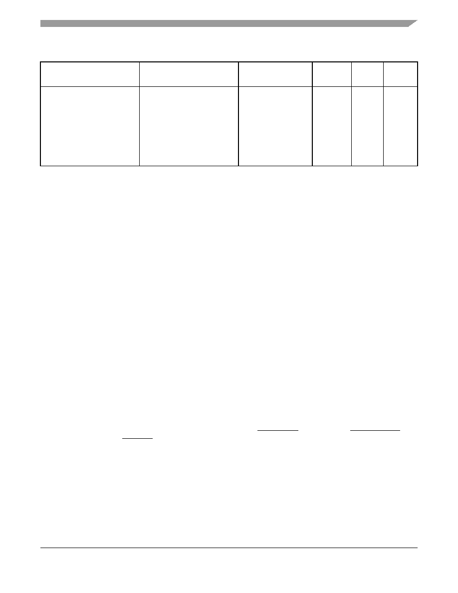
Package Description
N/C
No Connection
A16, A20, B16, B17,
B19, B20, C17, C18,
C19, D28, R31, T17,
V23, W23, Y22, Y23,
Y24, AA24, AB24,
AC24, AC26, AC27,
AC29, AD31, AE29,
AJ25, AK28, AL31,
AM21
——
17
Note:
1. All multiplexed signals are listed only once and do not re-occur. For example, LCS5/DMA_REQ2 is listed only once in the
local bus controller section, and is not mentioned in the DMA section even though the pin also functions as DMA_REQ2.
2. Recommend a weak pull-up resistor (2–10 K
Ω) be placed on this pin to OVDD.
4. This pin is an open drain signal.
5. This pin is a reset configuration pin. It has a weak internal pull-up P-FET which is enabled only when the processor is in the
reset state. This pull-up is designed such that it can be overpowered by an external 4.7-kO pull-down resistor. However, if the
signal is intended to be high after reset, and if there is any device on the net which might pull down the value of the net at
reset, then a pullup or active driver is needed.
6. Treat these pins as no connects (NC) unless using debug address functionality.
7. The value of LA[29:31] during reset sets the CCB clock to SYSCLK PLL ratio. These pins require 4.7-k
Ω pull-up or pull-down
resistors. See Section 19.2, “CCB/SYSCLK PLL Ratio.”
8. The value of LALE, LGPL2 and LBCTL at reset set the e500 core clock to CCB Clock PLL ratio. These pins require 4.7-k
Ω
pull-up or pull-down resistors. See the Section 19.3, “e500 Core PLL Ratio.”
9. Functionally, this pin is an output, but structurally it is an I/O because it either samples configuration input during reset or
because it has other manufacturing test functions. This pin therefore be described as an I/O for boundary scan.
10. If this pin is configured for local bus controller usage, recommend a weak pull-up resistor (2-10 K
Ω) be placed on this pin to
BVDD, to ensure no random chip select assertion due to possible noise and so on.
11. This output is actively driven during reset rather than being three-stated during reset.
12. These JTAG pins have weak internal pull-up P-FETs that are always enabled.
13. These pins are connected to the VDD/GND planes internally and may be used by the core power supply to improve tracking
and regulation.
14. Internal thermally sensitive diode.
15. If this pin is connected to a device that pulls down during reset, an external pull-up is required to drive this pin to a safe state
during reset.
16. This pin is only an output in FIFO mode when used as Rx Flow Control.
17. Do not connect.
18. These are test signals for factory use only and must be pulled up (100
Ω - 1 KΩ) to OVDD for normal machine operation.
19. Independent supplies derived from board VDD.
20. Recommend a pull-up resistor (~1 K
Ω) be placed on this pin to OVDD.
21. The following pins must NOT be pulled down during power-on reset: DMA1_DACK[0:1], EC5_MDC, HRESET_REQ,
TRIG_OUT/READY_P0/QUIESCE, MSRCID[2:4], MDVAL, ASLEEP.
22. This pin requires an external 4.7-k
Ω pull-down resistor to prevent PHY from seeing a valid Transmit Enable before it is
actively driven.
23. This pin is only an output in eTSEC3 FIFO mode when used as Rx flow control.
24. TSEC2_TXD[1] is used as cfg_dram_type. IT MUST BE VALID AT POWER-UP, EVEN BEFORE HRESET ASSERTION.
Table 76. MPC8572E Pinout Listing (continued)
Signal
Signal Name
Package Pin Number
Pin Type
Power
Supply
Notes
相关PDF资料 |
PDF描述 |
|---|---|
| MPC8548EVTAVHB | MPU POWERQUICC III 783-PBGA |
| MPC8548EPXAVHB | MPU POWERQUICC III 783-PBGA |
| XC4028XL-2BG352C | IC FPGA C-TEMP 3.3V 2SPD 352MBGA |
| XC4028XL-2BG256I | IC FPGA I-TEMP 3.3V 2SPD 256PBGA |
| FMC40DRYH-S93 | CONN EDGECARD 80POS .100 DIP SLD |
相关代理商/技术参数 |
参数描述 |
|---|---|
| MPC8572CLVTAULE | 功能描述:微处理器 - MPU R211 NoE NoPb 1333LP Ext RoHS:否 制造商:Atmel 处理器系列:SAMA5D31 核心:ARM Cortex A5 数据总线宽度:32 bit 最大时钟频率:536 MHz 程序存储器大小:32 KB 数据 RAM 大小:128 KB 接口类型:CAN, Ethernet, LIN, SPI,TWI, UART, USB 工作电源电压:1.8 V to 3.3 V 最大工作温度:+ 85 C 安装风格:SMD/SMT 封装 / 箱体:FBGA-324 |
| MPC8572CLVTAVND | 功能描述:微处理器 - MPU 1500 ExtTmp LwPwr RoHS:否 制造商:Atmel 处理器系列:SAMA5D31 核心:ARM Cortex A5 数据总线宽度:32 bit 最大时钟频率:536 MHz 程序存储器大小:32 KB 数据 RAM 大小:128 KB 接口类型:CAN, Ethernet, LIN, SPI,TWI, UART, USB 工作电源电压:1.8 V to 3.3 V 最大工作温度:+ 85 C 安装风格:SMD/SMT 封装 / 箱体:FBGA-324 |
| MPC8572CLVTAVNE | 功能描述:微处理器 - MPU R211 NoE NoPb 1500LP Ext RoHS:否 制造商:Atmel 处理器系列:SAMA5D31 核心:ARM Cortex A5 数据总线宽度:32 bit 最大时钟频率:536 MHz 程序存储器大小:32 KB 数据 RAM 大小:128 KB 接口类型:CAN, Ethernet, LIN, SPI,TWI, UART, USB 工作电源电压:1.8 V to 3.3 V 最大工作温度:+ 85 C 安装风格:SMD/SMT 封装 / 箱体:FBGA-324 |
| MPC8572CVTAVNE | 功能描述:微处理器 - MPU R211 NoE NoPb 1500 Ext RoHS:否 制造商:Atmel 处理器系列:SAMA5D31 核心:ARM Cortex A5 数据总线宽度:32 bit 最大时钟频率:536 MHz 程序存储器大小:32 KB 数据 RAM 大小:128 KB 接口类型:CAN, Ethernet, LIN, SPI,TWI, UART, USB 工作电源电压:1.8 V to 3.3 V 最大工作温度:+ 85 C 安装风格:SMD/SMT 封装 / 箱体:FBGA-324 |
| MPC8572DS | 功能描述:开发板和工具包 - 其他处理器 MICRO-ATX HIGH PERFORMAN RoHS:否 制造商:Freescale Semiconductor 产品:Development Systems 工具用于评估:P3041 核心:e500mc 接口类型:I2C, SPI, USB 工作电源电压: |
发布紧急采购,3分钟左右您将得到回复。