- 您现在的位置:买卖IC网 > PDF目录4036 > MPC8572CLVTAULD (Freescale Semiconductor)MPU POWERQUICC III 1023-PBGA PDF资料下载
参数资料
| 型号: | MPC8572CLVTAULD |
| 厂商: | Freescale Semiconductor |
| 文件页数: | 66/138页 |
| 文件大小: | 0K |
| 描述: | MPU POWERQUICC III 1023-PBGA |
| 标准包装: | 1 |
| 系列: | MPC85xx |
| 处理器类型: | 32-位 MPC85xx PowerQUICC III |
| 速度: | 1.333GHz |
| 电压: | 1.1V |
| 安装类型: | 表面贴装 |
| 封装/外壳: | 1023-BBGA,FCBGA |
| 供应商设备封装: | 1023-FCPBGA(33x33) |
| 包装: | 托盘 |
第1页第2页第3页第4页第5页第6页第7页第8页第9页第10页第11页第12页第13页第14页第15页第16页第17页第18页第19页第20页第21页第22页第23页第24页第25页第26页第27页第28页第29页第30页第31页第32页第33页第34页第35页第36页第37页第38页第39页第40页第41页第42页第43页第44页第45页第46页第47页第48页第49页第50页第51页第52页第53页第54页第55页第56页第57页第58页第59页第60页第61页第62页第63页第64页第65页当前第66页第67页第68页第69页第70页第71页第72页第73页第74页第75页第76页第77页第78页第79页第80页第81页第82页第83页第84页第85页第86页第87页第88页第89页第90页第91页第92页第93页第94页第95页第96页第97页第98页第99页第100页第101页第102页第103页第104页第105页第106页第107页第108页第109页第110页第111页第112页第113页第114页第115页第116页第117页第118页第119页第120页第121页第122页第123页第124页第125页第126页第127页第128页第129页第130页第131页第132页第133页第134页第135页第136页第137页第138页
MPC8572E PowerQUICC III Integrated Processor Hardware Specifications, Rev. 5
Freescale Semiconductor
33
Ethernet: Enhanced Three-Speed Ethernet (eTSEC)
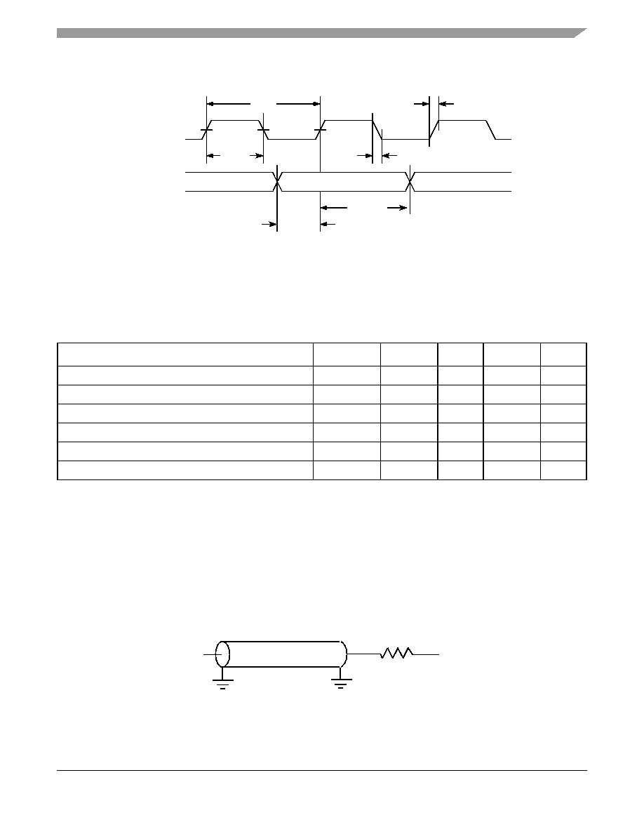
Figure 9 shows the GMII transmit AC timing diagram.
Figure 9. GMII Transmit AC Timing Diagram
8.2.2.2
GMII Receive AC Timing Specifications
Table 28 provides the GMII receive AC timing specifications.
Figure 10 provides the AC test load for eTSEC.
Figure 10. eTSEC AC Test Load
Table 28. GMII Receive AC Timing Specifications
At recommended operating conditions with LVDD/TVDD of 2.5/ 3.3 V ± 5%.
Parameter/Condition
Symbol 1
Min
Typ
Max
Unit
RX_CLK clock period
tGRX
—8.0
—
ns
RX_CLK duty cycle
tGRXH/tGRX
40
—
60
ns
RXD[7:0], RX_DV, RX_ER setup time to RX_CLK
tGRDVKH
2.0
—
ns
RXD[7:0], RX_DV, RX_ER hold time to RX_CLK
tGRDXKH
0—
—
ns
RX_CLK clock rise (20%-80%)
tGRXR
2
——
1.0
ns
RX_CLK clock fall time (80%-20%)
tGRXF
2
——
1.0
ns
Note:
1. The symbols used for timing specifications herein follow the pattern of t(first two letters of functional block)(signal)(state) (reference)(state)
for inputs and t(first two letters of functional block)(reference)(state)(signal)(state) for outputs. For example, tGRDVKH symbolizes GMII
receive timing (GR) with respect to the time data input signals (D) reaching the valid state (V) relative to the tRX clock
reference (K) going to the high state (H) or setup time. Also, tGRDXKL symbolizes GMII receive timing (GR) with respect to
the time data input signals (D) went invalid (X) relative to the tGRX clock reference (K) going to the low (L) state or hold time.
Note that, in general, the clock reference symbol representation is based on three letters representing the clock of a particular
functional. For example, the subscript of tGRX represents the GMII (G) receive (RX) clock. For rise and fall times, the latter
convention is used with the appropriate letter: R (rise) or F (fall).
2. Guaranteed by design.
GTX_CLK
TXD[7:0]
tGTKHDX
tGTX
tGTXH
tGTXR
tGTXF
tGTKHDV
TX_EN
TX_ER
Output
LVDD/2
RL = 50 Ω
Z0 = 50 Ω
相关PDF资料 |
PDF描述 |
|---|---|
| MPC8548EVTAVHB | MPU POWERQUICC III 783-PBGA |
| MPC8548EPXAVHB | MPU POWERQUICC III 783-PBGA |
| XC4028XL-2BG352C | IC FPGA C-TEMP 3.3V 2SPD 352MBGA |
| XC4028XL-2BG256I | IC FPGA I-TEMP 3.3V 2SPD 256PBGA |
| FMC40DRYH-S93 | CONN EDGECARD 80POS .100 DIP SLD |
相关代理商/技术参数 |
参数描述 |
|---|---|
| MPC8572CLVTAULE | 功能描述:微处理器 - MPU R211 NoE NoPb 1333LP Ext RoHS:否 制造商:Atmel 处理器系列:SAMA5D31 核心:ARM Cortex A5 数据总线宽度:32 bit 最大时钟频率:536 MHz 程序存储器大小:32 KB 数据 RAM 大小:128 KB 接口类型:CAN, Ethernet, LIN, SPI,TWI, UART, USB 工作电源电压:1.8 V to 3.3 V 最大工作温度:+ 85 C 安装风格:SMD/SMT 封装 / 箱体:FBGA-324 |
| MPC8572CLVTAVND | 功能描述:微处理器 - MPU 1500 ExtTmp LwPwr RoHS:否 制造商:Atmel 处理器系列:SAMA5D31 核心:ARM Cortex A5 数据总线宽度:32 bit 最大时钟频率:536 MHz 程序存储器大小:32 KB 数据 RAM 大小:128 KB 接口类型:CAN, Ethernet, LIN, SPI,TWI, UART, USB 工作电源电压:1.8 V to 3.3 V 最大工作温度:+ 85 C 安装风格:SMD/SMT 封装 / 箱体:FBGA-324 |
| MPC8572CLVTAVNE | 功能描述:微处理器 - MPU R211 NoE NoPb 1500LP Ext RoHS:否 制造商:Atmel 处理器系列:SAMA5D31 核心:ARM Cortex A5 数据总线宽度:32 bit 最大时钟频率:536 MHz 程序存储器大小:32 KB 数据 RAM 大小:128 KB 接口类型:CAN, Ethernet, LIN, SPI,TWI, UART, USB 工作电源电压:1.8 V to 3.3 V 最大工作温度:+ 85 C 安装风格:SMD/SMT 封装 / 箱体:FBGA-324 |
| MPC8572CVTAVNE | 功能描述:微处理器 - MPU R211 NoE NoPb 1500 Ext RoHS:否 制造商:Atmel 处理器系列:SAMA5D31 核心:ARM Cortex A5 数据总线宽度:32 bit 最大时钟频率:536 MHz 程序存储器大小:32 KB 数据 RAM 大小:128 KB 接口类型:CAN, Ethernet, LIN, SPI,TWI, UART, USB 工作电源电压:1.8 V to 3.3 V 最大工作温度:+ 85 C 安装风格:SMD/SMT 封装 / 箱体:FBGA-324 |
| MPC8572DS | 功能描述:开发板和工具包 - 其他处理器 MICRO-ATX HIGH PERFORMAN RoHS:否 制造商:Freescale Semiconductor 产品:Development Systems 工具用于评估:P3041 核心:e500mc 接口类型:I2C, SPI, USB 工作电源电压: |
发布紧急采购,3分钟左右您将得到回复。