- 您现在的位置:买卖IC网 > PDF目录2099 > MPC9229EI (IDT, Integrated Device Technology Inc)IC CLK SYNTH LV PECL 28-PLCC PDF资料下载
参数资料
| 型号: | MPC9229EI |
| 厂商: | IDT, Integrated Device Technology Inc |
| 文件页数: | 1/14页 |
| 文件大小: | 0K |
| 描述: | IC CLK SYNTH LV PECL 28-PLCC |
| 标准包装: | 37 |
| 类型: | 时钟/频率合成器 |
| PLL: | 带旁路 |
| 输入: | 晶体 |
| 输出: | LVPECL |
| 电路数: | 1 |
| 比率 - 输入:输出: | 1:1 |
| 差分 - 输入:输出: | 无/是 |
| 频率 - 最大: | 400MHz |
| 除法器/乘法器: | 是/无 |
| 电源电压: | 3.135 V ~ 3.465 V |
| 工作温度: | 0°C ~ 70°C |
| 安装类型: | 表面贴装 |
| 封装/外壳: | 28-LCC(J 形引线) |
| 供应商设备封装: | 28-PLCC(11.5x11.5) |
| 包装: | 管件 |
DATA SHEET
MPC9229 REVISION 5 DECEMBER 19, 2012
1
2012 Integrated Device Technology, Inc.
400MHz Low Voltage PECL Clock Synthesizer
MPC9229
The MPC9229 is a 3.3 V compatible, PLL based clock synthesizer targeted for high
performance clock generation in mid-range to high-performance telecom, networking and
computing applications. With output frequencies from 25 MHz to 400 MHz and the support of
differential PECL output signals the device meets the needs of the most demanding clock
applications.
Features
25 MHz to 400 MHz Synthesized Clock Output Signal
Differential PECL Output
LVCMOS Compatible Control Inputs
On-Chip Crystal Oscillator for Reference Frequency Generation
3.3-V Power Supply
Fully Integrated PLL
Minimal Frequency Overshoot
Serial 3-Wire Programming Interface
Parallel Programming Interface for Power-Up
32-Lead LQFP and 28-Lead PLCC Packaging
32-Lead and 28-Lead Pb-Free Package
SiGe Technology
Ambient Temperature Range 0°C to +70°C
Pin and Function Compatible to the MC12429
Replacement part: ICS84329B
Functional Description
The internal crystal oscillator uses the external quartz crystal as the basis of its frequency
reference. The frequency of the internal crystal oscillator is divided by 16 and then multiplied
by the PLL. The VCO within the PLL operates over a range of 800 to 1600 MHz. Its output is
scaled by a divider that is configured by either the serial or parallel interfaces. The crystal
oscillator frequency fXTAL, the PLL feedback-divider M and the PLL post-divider N determine
the output frequency.
The feedback path of the PLL is internal. The PLL adjusts the VCO output frequency to be
4
M times the reference frequency by adjusting the VCO control voltage. Note that for some
values of M (either too high or too low) the PLL will not achieve phase lock. The PLL will be stable if the VCO frequency is within the specified
VCO frequency range (800 to 1600 MHz). The M-value must be programmed by the serial or parallel interface.
The PLL post-divider N is configured through either the serial or the parallel interfaces, and can provide one of four division ratios (1, 2, 4,
or 8). This divider extends performance of the part while providing a 50% duty cycle. The output driver is driven differentially from the output
divider, and is capable of driving a pair of transmission lines terminated 50
to VCC –2.0 V. The positive supply voltage for the internal PLL
is separated from the power supply for the core logic and output drivers to minimize noise induced jitter.
The configuration logic has two sections: serial and parallel. The parallel interface uses the values at the M[8:0] and N[1:0] inputs to configure
the internal counters. It is recommended on system reset to hold the P_LOAD input LOW until power becomes valid. On the LOW-to-HIGH
transition of P_LOAD, the parallel inputs are captured. The parallel interface has priority over the serial interface. Internal pullup resistors are
provided on the M[8:0] and N[1:0] inputs prevent the LVCMOS compatible control inputs from floating.
The serial interface centers on a fourteen bit shift register. The shift register shifts once per rising edge of the S_CLOCK input. The serial
input S_DATA must meet setup and hold timing as specified in the AC Characteristics section of this document. The configuration latches will
capture the value of the shift register on the HIGH-to-LOW edge of the S_LOAD input. Refer to Programming Interface for more information.
The TEST output reflects various internal node values, and is controlled by the T[2:0] bits in the serial data stream. In order to minimize the
PLL jitter, it is recommended to avoid active signal on the TEST output.
MPC9229
400 MHz LOW VOLTAGE
CLOCK SYNTHESIZER
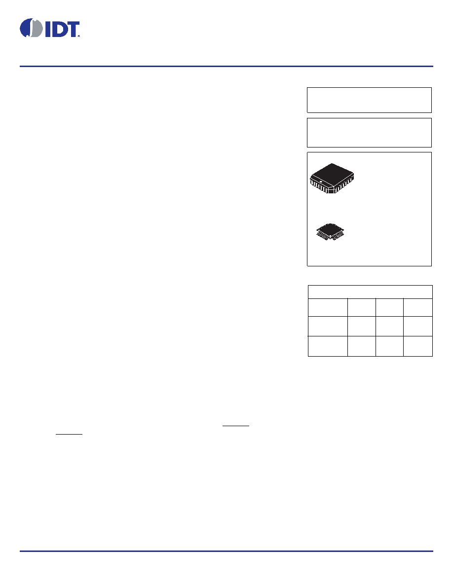
ORDERING INFORMATION
Device
Temp.
Range
Case
No.
Package
MPC9229EI
0°C
to +70°C
776-02
PLCC
MPC9229AC
0°C
to +70°C
873A-03
LQFP
AC SUFFIX
32-LEAD LQFP PACKAGE
Pb-FREE PACKAGE
CASE 873A-04
EI SUFFIX
28-LEAD PLCC PACKAGE
Pb-FREE PACKAGE
CASE 776-02
PRODUCT DISCONTINUANCE NOTICE - LAST TIME BUY EXPIRES ON (12/3/13)
相关PDF资料 |
PDF描述 |
|---|---|
| MPC92429EI | IC SYNTHESIZER LVPECL 28-PLCC |
| MPC92469AC | IC SYNTHESIZER LVPECL 32-LQFP |
| MPC9315AC | IC PLL CLOCK GEN/DRIVER 32-LQFP |
| MPC9350AC | IC PLL CLOCK DRIVER LV 32-LQFP |
| MPC941AE | IC CLOCK BUFFER MUX 1:27 48-LQFP |
相关代理商/技术参数 |
参数描述 |
|---|---|
| MPC9229EIR2 | 功能描述:时钟合成器/抖动清除器 FSL 400MHz LVPECL Freq. Synthesizer RoHS:否 制造商:Skyworks Solutions, Inc. 输出端数量: 输出电平: 最大输出频率: 输入电平: 最大输入频率:6.1 GHz 电源电压-最大:3.3 V 电源电压-最小:2.7 V 封装 / 箱体:TSSOP-28 封装:Reel |
| MPC9229FA | 功能描述:IC PECL CLOCK LV 400MHZ 32-LQFP RoHS:否 类别:集成电路 (IC) >> 时钟/计时 - 时钟发生器,PLL,频率合成器 系列:- 标准包装:39 系列:- 类型:* PLL:带旁路 输入:时钟 输出:时钟 电路数:1 比率 - 输入:输出:1:10 差分 - 输入:输出:是/是 频率 - 最大:170MHz 除法器/乘法器:无/无 电源电压:2.375 V ~ 3.465 V 工作温度:0°C ~ 70°C 安装类型:* 封装/外壳:* 供应商设备封装:* 包装:* |
| MPC9229FAR2 | 制造商:Integrated Device Technology Inc 功能描述:PLL Clock Synthesizer Single 32-Pin TQFP T/R |
| MPC9229FN | 功能描述:锁相环 - PLL 3.3V 400MHz Clock Generator RoHS:否 制造商:Silicon Labs 类型:PLL Clock Multiplier 电路数量:1 最大输入频率:710 MHz 最小输入频率:0.002 MHz 输出频率范围:0.002 MHz to 808 MHz 电源电压-最大:3.63 V 电源电压-最小:1.71 V 最大工作温度:+ 85 C 最小工作温度:- 40 C 封装 / 箱体:QFN-36 封装:Tray |
| MPC9229FNR2 | 制造商:Integrated Device Technology Inc 功能描述:PLL Clock Synthesizer Single 28-Pin PLCC T/R |
发布紧急采购,3分钟左右您将得到回复。