- 您现在的位置:买卖IC网 > PDF目录2099 > MPC9229EI (IDT, Integrated Device Technology Inc)IC CLK SYNTH LV PECL 28-PLCC PDF资料下载
参数资料
| 型号: | MPC9229EI |
| 厂商: | IDT, Integrated Device Technology Inc |
| 文件页数: | 12/14页 |
| 文件大小: | 0K |
| 描述: | IC CLK SYNTH LV PECL 28-PLCC |
| 标准包装: | 37 |
| 类型: | 时钟/频率合成器 |
| PLL: | 带旁路 |
| 输入: | 晶体 |
| 输出: | LVPECL |
| 电路数: | 1 |
| 比率 - 输入:输出: | 1:1 |
| 差分 - 输入:输出: | 无/是 |
| 频率 - 最大: | 400MHz |
| 除法器/乘法器: | 是/无 |
| 电源电压: | 3.135 V ~ 3.465 V |
| 工作温度: | 0°C ~ 70°C |
| 安装类型: | 表面贴装 |
| 封装/外壳: | 28-LCC(J 形引线) |
| 供应商设备封装: | 28-PLCC(11.5x11.5) |
| 包装: | 管件 |
MPC9229 REVISION 5 DECEMBER 19, 2012
7
2012 Integrated Device Technology, Inc.
MPC9229 Data Sheet
400MHZ LOW VOLTAGE PECL CLOCK SYNTHESIZER
Substituting N for the four available values for N (1, 2, 4, 8) yields:
Example Frequency Calculation for an 16 MHz Input Frequency
If an output frequency of 131 MHz was desired the following steps
would be taken to identify the appropriate M and N values.
According to Table 8., 131 MHz falls in the frequency set by an value
of 2 so N[1:0] = 01. For N = 2 the output frequency is fOUT = M 2
and M = fOUT x 2. Therefore M = 2 x 131 = 262, so M[8:0] =
100000110. Following this procedure a user can generate any whole
frequency between 25 MHz and 400 MHz. Note than for N > 2
fractional values of can be realized. The size of the programmable
frequency steps (and thus the indicator of the fractional output
frequencies achievable) will be equal to:
fSTEP = fXTAL 16 N
APPLICATIONS INFORMATION
Using the Parallel and Serial Interface
The M and N counters can be loaded either through a parallel or
serial interface. The parallel interface is controlled via the P_LOAD
signal such that a LOW-to-HIGH transition will latch the information
present on the M[8:0] and N[1:0] inputs into the M and N counters.
When the P_LOAD signal is LOW, the input latches will be
transparent and any changes on the M[8:0] and N[1:0] inputs will
affect the fOUT output pair. To use the serial port, the S_CLOCK
signal samples the information on the S_DATA line and loads it into
a 14-bit shift register. Note that the P_LOAD signal must be HIGH
for the serial load operation to function. The Test register is loaded
with the first three bits, the N register with the next two and the M
register with the final eight bits of the data stream on the S_DATA
input. For each register the most significant bit is loaded first (T2, N1,
and M8). A pulse on the S_LOAD pin after the shift register is fully
loaded will transfer the divide values into the counters. The HIGH-
to-LOW transition on the S_LOAD input will latch the new divide
values into the counters. Figure 3. illustrates the timing diagram for
both a parallel and a serial load of the MPC9229 synthesizer. M[8:0]
and N[1:0] are normally specified once at power-up through the
parallel interface, and then possibly again through the serial
interface. This approach allows the application to come up at one
frequency and then change or fine-tune the clock as the ability to
control the serial interface becomes available.
Using the Test and Diagnosis Output TEST
The TEST output provides visibility for one of the several internal
nodes as determined by the T[2:0] bits in the serial configuration
stream. It is not configurable through the parallel interface. Although
it is possible to select the node that represents fOUT, the CMOS
output is not able to toggle fast enough for higher output frequencies
and should only be used for test and diagnosis. The T2, T1, and T0
control bits are preset to ‘000' when P_LOAD is LOW so that the
PECL fOUT outputs are as jitter-free as possible. Any active signal
on the TEST output pin will have detrimental affects on the jitter of
the PECL output pair. In normal operations, jitter specifications are
only guaranteed if the TEST output is static. The serial configuration
port can be used to select one of the alternate functions for this pin.
Most of the signals available on the TEST output pin are useful only
for performance verification of the MPC9229 itself. However the PLL
bypass mode may be of interest at the board level for functional
debug. When T[2:0] is set to 110, the MPC9229 is placed in PLL
bypass mode. In this mode the S_CLOCK input is fed directly into
the M and N dividers. The N divider drives the fOUT differential pair
and the M counter drives the TEST output pin. In this mode the
S_CLOCK input could be used for low speed board level functional
test or debug. Bypassing the PLL and driving fOUT directly gives the
user more control on the test clocks sent through the clock tree.
Figure 5. shows the functional setup of the PLL bypass mode.
Because the S_CLOCK is a CMOS level, the input frequency is
limited to 200 MHz. This means the fastest the fOUT pin can be
toggled via the S_CLOCK is 100 MHz as the divide ratio of the
Post-PLL divider is 2 (if N = 1). Note that the M counter output on the
TEST output will not be a 50% duty cycle.
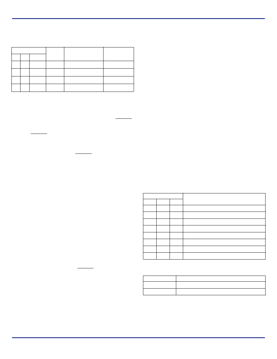
Table 8. Output Frequency Range for fXTAL = 16 MHz
N
fOUT
fOUT Range
fOUT Step
1
0
Value
0
1
M
200 – 400 MHz
1 MHz
0
1
2
M
2
100 – 200 MHz
500 kHz
1
0
4
M
4
50 – 100 MHz
250 kHz
1
8
M
8
25 – 50 MHz
125 kHz
Table 9. Test and Debug Configuration for TEST
T[2:0]
TEST Output
T2
T1
T0
0
14-bit shift register out(1)
1. Clocked out at the rate of S_CLOCK
0
1
Logic 1
0
1
0
fXTAL 16
0
1
M-Counter out
1
0
fOUT
1
0
1
Logic 0
1
0
M-Counter out in PLL-bypass mode
1
fOUT 4
Table 10. Debug Configuration for PLL Bypass(1)
1. T[2:0] = 110. AC specifications do not apply in PLL bypass mode
Output
Configuration
fOUT
S_CLOCK
N
TEST
M-Counter out(2)
2. Clocked out at the rate of S_CLOCK
(4 N)
相关PDF资料 |
PDF描述 |
|---|---|
| MPC92429EI | IC SYNTHESIZER LVPECL 28-PLCC |
| MPC92469AC | IC SYNTHESIZER LVPECL 32-LQFP |
| MPC9315AC | IC PLL CLOCK GEN/DRIVER 32-LQFP |
| MPC9350AC | IC PLL CLOCK DRIVER LV 32-LQFP |
| MPC941AE | IC CLOCK BUFFER MUX 1:27 48-LQFP |
相关代理商/技术参数 |
参数描述 |
|---|---|
| MPC9229EIR2 | 功能描述:时钟合成器/抖动清除器 FSL 400MHz LVPECL Freq. Synthesizer RoHS:否 制造商:Skyworks Solutions, Inc. 输出端数量: 输出电平: 最大输出频率: 输入电平: 最大输入频率:6.1 GHz 电源电压-最大:3.3 V 电源电压-最小:2.7 V 封装 / 箱体:TSSOP-28 封装:Reel |
| MPC9229FA | 功能描述:IC PECL CLOCK LV 400MHZ 32-LQFP RoHS:否 类别:集成电路 (IC) >> 时钟/计时 - 时钟发生器,PLL,频率合成器 系列:- 标准包装:39 系列:- 类型:* PLL:带旁路 输入:时钟 输出:时钟 电路数:1 比率 - 输入:输出:1:10 差分 - 输入:输出:是/是 频率 - 最大:170MHz 除法器/乘法器:无/无 电源电压:2.375 V ~ 3.465 V 工作温度:0°C ~ 70°C 安装类型:* 封装/外壳:* 供应商设备封装:* 包装:* |
| MPC9229FAR2 | 制造商:Integrated Device Technology Inc 功能描述:PLL Clock Synthesizer Single 32-Pin TQFP T/R |
| MPC9229FN | 功能描述:锁相环 - PLL 3.3V 400MHz Clock Generator RoHS:否 制造商:Silicon Labs 类型:PLL Clock Multiplier 电路数量:1 最大输入频率:710 MHz 最小输入频率:0.002 MHz 输出频率范围:0.002 MHz to 808 MHz 电源电压-最大:3.63 V 电源电压-最小:1.71 V 最大工作温度:+ 85 C 最小工作温度:- 40 C 封装 / 箱体:QFN-36 封装:Tray |
| MPC9229FNR2 | 制造商:Integrated Device Technology Inc 功能描述:PLL Clock Synthesizer Single 28-Pin PLCC T/R |
发布紧急采购,3分钟左右您将得到回复。