- 您现在的位置:买卖IC网 > PDF目录2099 > MPC961CAC (IDT, Integrated Device Technology Inc)IC BUFFER ZD 1:18 PLL 32-LQFP PDF资料下载
参数资料
| 型号: | MPC961CAC |
| 厂商: | IDT, Integrated Device Technology Inc |
| 文件页数: | 9/11页 |
| 文件大小: | 0K |
| 描述: | IC BUFFER ZD 1:18 PLL 32-LQFP |
| 标准包装: | 250 |
| 类型: | 零延迟缓冲器 |
| PLL: | 是 |
| 输入: | LVCMOS |
| 输出: | LVCMOS |
| 电路数: | 1 |
| 比率 - 输入:输出: | 1:17 |
| 差分 - 输入:输出: | 无/无 |
| 频率 - 最大: | 200MHz |
| 除法器/乘法器: | 无/无 |
| 电源电压: | 2.375 V ~ 3.465 V |
| 工作温度: | -40°C ~ 85°C |
| 安装类型: | 表面贴装 |
| 封装/外壳: | 32-LQFP |
| 供应商设备封装: | 32-TQFP(7x7) |
| 包装: | 托盘 |
MPC961C Data Sheet
LOW VOLTAGE ZERO DELAY BUFFER
MPC961C REVISION 5 AUGUST 17, 2009
7
2009 Integrated Device Technology, Inc.
The feedback trace delay is determined by the board layout and
can be used to fine-tune the effective delay through each device. In
the following example calculation a
I/O jitter confidence factor of 99.7% (
± 3σ) is assumed, resulting in
a worst case timing uncertainty from input to any output of -275 ps
to 315 ps relative to CCLK:
tSK(PP) = [-80ps...120ps] + [-150ps...150ps] +
[(15ps @ -3)...(15ps @ 3)] + tPD, LINE(FB)
tSK(PP) = [-275ps...315ps] + tPD, LINE(FB)
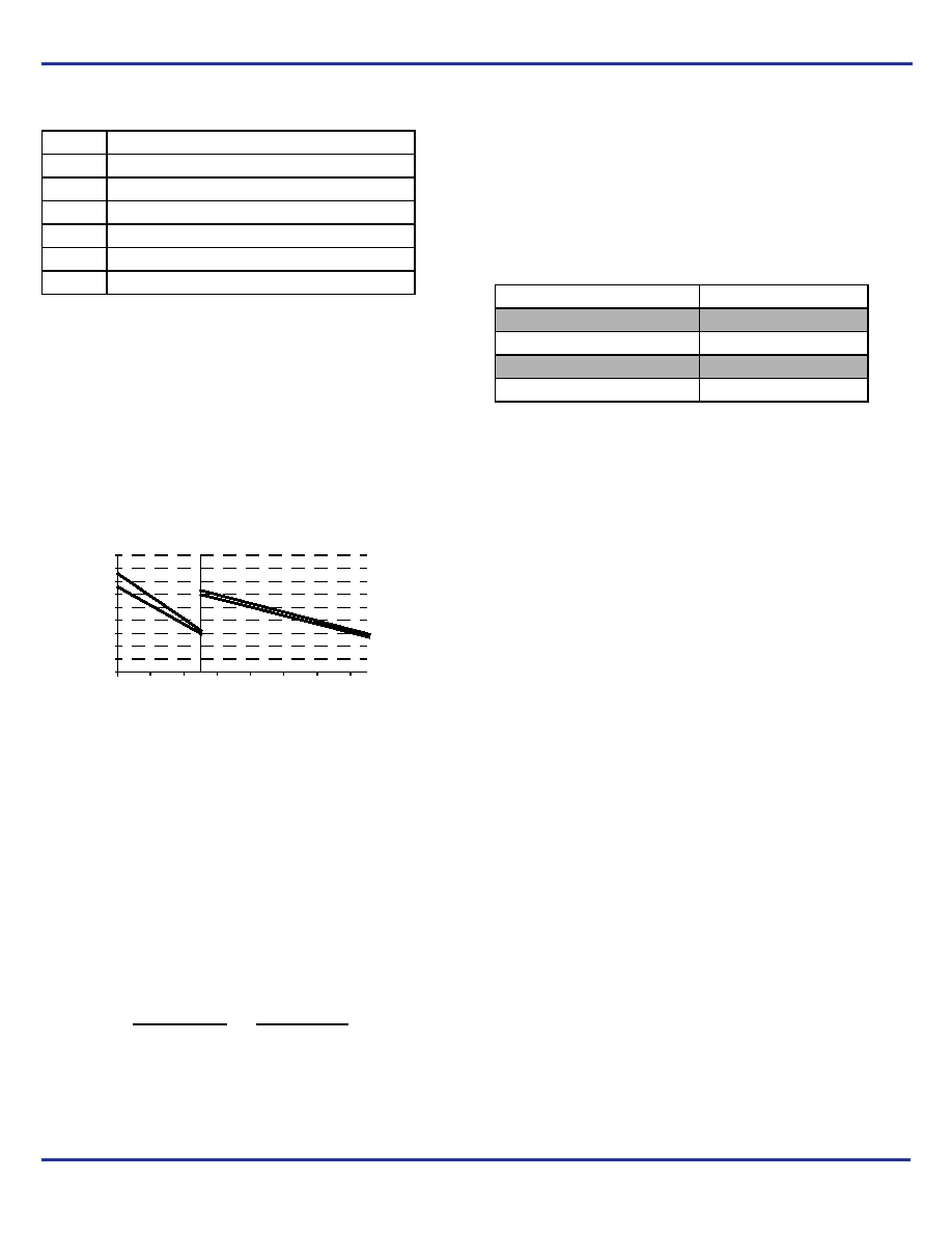
Due to the frequency dependence of the I/O jitter, Figure 8 can be
used for a more precise timing performance analysis.
Figure 8. Max. I/O Jitter versus Frequency
Power Consumption of the MPC961C and Thermal
Management
The MPC961C AC specification is guaranteed for the entire
operating frequency range up to 200 MHz. The MPC961C power
consumption and the associated long-term reliability may decrease
the maximum frequency limit, depending on operating conditions
such as clock frequency, supply voltage, output loading, ambient
temperature, vertical convection and thermal conductivity of
package and board. This section describes the impact of these
parameters on the junction temperature and gives a guideline to
estimate the MPC961C die junction temperature and the associated
device reliability. For a complete analysis of power consumption as
a function of operating conditions and associated long term device
reliability refer to the Application Note AN1545. According the
AN1545, the long-term device reliability is a function of the die
junction temperature:
Increased power consumption will increase the die junction
temperature and impact the device reliability (MTBF). According to
the system-defined tolerable MTBF, the die junction temperature of
the MPC961C needs to be controlled and the thermal impedance of
the board/package should be optimized. The power dissipated in the
MPC961C is represented in equation 1.
Where ICCQ is the static current consumption of the MPC961C,
CPD is the power dissipation capacitance per output, (Μ)ΣCL
represents the external capacitive output load, N is the number of
active outputs (N is always 27 in case of the MPC961C). The
MPC961C supports driving transmission lines to maintain high
signal integrity and tight timing parameters. Any transmission line
will hide the lumped capacitive load at the end of the board trace,
therefore,
ΣCL is zero for controlled transmission line systems and
can be eliminated from equation 1. Using parallel termination output
termination results in equation 2 for power dissipation.
In equation 2, P stands for the number of outputs with a parallel
or thevenin termination, VOL, IOL, VOH, and IOH are a function of the
output termination technique and DCQ is the clock signal duty cycle.
If transmission lines are used
ΣCL is zero in equation 2 and can be
eliminated. In general, the use of controlled transmission line
techniques eliminates the impact of the lumped capacitive loads at
the end lines and greatly reduces the power dissipation of the
device. Equation 3 describes the die junction temperature TJ as a
function of the power consumption.
Table 8. Confidence Factor CF
CF
Probability of clock edge within the distribution
± 1σ
0.68268948
± 2σ
0.95449988
± 3σ
0.99730007
± 4σ
0.99993663
± 5σ
0.99999943
± 6σ
0.99999999
F_RANGE = 1
F_RANGE = 0
18
16
14
12
10
8
6
4
2
0
50
70
90
110
130
150
170
190
Clock frequency [MHz]
t jit(
φ)
[p
s]
RMS
Table 9. Die Junction Temperature and MTBF
Junction Temperature (
°C)
MTBF (Years)
100
20.4
110
9.1
120
4.2
130
2.0
PTOT = [ ICCQ + VCC fCLOCK ( N CPD + Σ CL ) ] VCC
M
PTOT = VCC [ ICCQ + VCC fCLOCK ( N CPD + Σ CL ) ] + Σ [ DCQ IOH (VCC – VOH) + (1 – DCQ) IOL VOL ]
M
P
TJ = TA + PTOT Rthja
fCLOCK,MAX =
CPD N V2CC
1
[
– (ICCQ VCC)
]
Rthja
Tj,MAX – TA
Equation 1
Equation 2
Equation 3
Equation 4
相关PDF资料 |
PDF描述 |
|---|---|
| MPC961PAC | IC BUFFER ZD 1:18 PLL 32-LQFP |
| MPC9653AAC | IC PLL CLK GEN 1:8 3.3V 32-LQFP |
| MPC9658AC | IC PLL CLK GEN 1:10 3.3V 32-LQFP |
| MPC9772FA | IC PLL CLK GEN 1:12 3.3V 52-LQFP |
| MPC9774FAR2 | IC PLL CLK GEN 1:14 3.3V 52-LQFP |
相关代理商/技术参数 |
参数描述 |
|---|---|
| MPC961CACR2 | 功能描述:IC BUFFER ZD 1:18 PLL 32-LQFP RoHS:是 类别:集成电路 (IC) >> 时钟/计时 - 时钟发生器,PLL,频率合成器 系列:- 标准包装:1,000 系列:- 类型:时钟/频率合成器,扇出分配 PLL:- 输入:- 输出:- 电路数:- 比率 - 输入:输出:- 差分 - 输入:输出:- 频率 - 最大:- 除法器/乘法器:- 电源电压:- 工作温度:- 安装类型:表面贴装 封装/外壳:56-VFQFN 裸露焊盘 供应商设备封装:56-VFQFP-EP(8x8) 包装:带卷 (TR) 其它名称:844S012AKI-01LFT |
| MPC961CFA | 功能描述:IC ZDB CMOS LV 1:18 32-LQFP RoHS:否 类别:集成电路 (IC) >> 时钟/计时 - 时钟发生器,PLL,频率合成器 系列:- 标准包装:39 系列:- 类型:* PLL:带旁路 输入:时钟 输出:时钟 电路数:1 比率 - 输入:输出:1:10 差分 - 输入:输出:是/是 频率 - 最大:170MHz 除法器/乘法器:无/无 电源电压:2.375 V ~ 3.465 V 工作温度:0°C ~ 70°C 安装类型:* 封装/外壳:* 供应商设备封装:* 包装:* |
| MPC961PAC | 功能描述:时钟缓冲器 RoHS:否 制造商:Texas Instruments 输出端数量:5 最大输入频率:40 MHz 传播延迟(最大值): 电源电压-最大:3.45 V 电源电压-最小:2.375 V 最大功率耗散: 最大工作温度:+ 85 C 最小工作温度:- 40 C 封装 / 箱体:LLP-24 封装:Reel |
| MPC961PACR2 | 功能描述:时钟缓冲器 RoHS:否 制造商:Texas Instruments 输出端数量:5 最大输入频率:40 MHz 传播延迟(最大值): 电源电压-最大:3.45 V 电源电压-最小:2.375 V 最大功率耗散: 最大工作温度:+ 85 C 最小工作温度:- 40 C 封装 / 箱体:LLP-24 封装:Reel |
| MPC961PFA | 功能描述:IC ZDB PECL LV 1:18 32-LQFP RoHS:否 类别:集成电路 (IC) >> 时钟/计时 - 时钟发生器,PLL,频率合成器 系列:- 标准包装:39 系列:- 类型:* PLL:带旁路 输入:时钟 输出:时钟 电路数:1 比率 - 输入:输出:1:10 差分 - 输入:输出:是/是 频率 - 最大:170MHz 除法器/乘法器:无/无 电源电压:2.375 V ~ 3.465 V 工作温度:0°C ~ 70°C 安装类型:* 封装/外壳:* 供应商设备封装:* 包装:* |
发布紧急采购,3分钟左右您将得到回复。