- 您现在的位置:买卖IC网 > PDF目录29137 > MPC9653FA (MOTOROLA INC) PLL BASED CLOCK DRIVER, 8 TRUE OUTPUT(S), 0 INVERTED OUTPUT(S), PQFP32 PDF资料下载
参数资料
| 型号: | MPC9653FA |
| 厂商: | MOTOROLA INC |
| 元件分类: | 时钟及定时 |
| 英文描述: | PLL BASED CLOCK DRIVER, 8 TRUE OUTPUT(S), 0 INVERTED OUTPUT(S), PQFP32 |
| 封装: | 7 X 7 MM, LQFP-32 |
| 文件页数: | 6/9页 |
| 文件大小: | 154K |
| 代理商: | MPC9653FA |
5
MPC9653
MOTOROLA ADVANCED CLOCK DRIVERS DEVICE DATA
514
APPLICATIONS INFORMATION
Programming the MPC9653
The MPC9653 supports output clock frequencies from 25 to
125 MHz. Two different feedback divider configurations can be
used to achieve the desired frequency operation range. The
feedback divider (VCO_SEL) should be used to situate the
VCO in the frequency lock range between 200 and 500 MHz
for stable and optimal operation. Two operating frequency
ranges are supported: 25 to 62.5 MHz and 50 to 125 MHz.
Table 9 illustrates the configurations supported by the
MPC9653. PLL zero-delay is supported if BYPASS=1,
PLL_EN=1 and the input frequency is within the specified PLL
reference frequency range.
Table 9: MPC9653 Configurations (QFB connected to FB_IN)
BYPAS
PLL_EN
VCO_SE
Operation
Frequency
S
_
L
p
Ratio
Output range (fQ0-7)
VCO
0
X
Test mode: PLL and divider bypass
fQ0-7 = fREF
0-200 MHz
n/a
1
0
Test mode: PLL bypass
fQ0-7 = fREF ÷ 4
0-50 MHz
n/a
1
0
1
Test mode: PLL bypass
fQ0-7 = fREF ÷ 8
0-25 MHz
n/a
1
0
PLL mode (high frequency range)
fQ0-7 = fREF
50 to 125 MHz
fVCO = fREF 4
1
PLL mode (low frequency range)
fQ0-7 = fREF
25 to 62.5 MHz
fVCO = fREF 8
Power Supply Filtering
The MPC9653 is a mixed analog/digital product. Its analog
circuitry is naturally susceptible to random noise, especially if
this noise is seen on the power supply pins. Random noise on
the VCCA_PLL power supply impacts the device characteristics,
for instance I/O jitter. The MPC9653 provides separate power
supplies for the output buffers (VCC) and the phase-locked
loop (VCCA_PLL) of the device. The purpose of this design tech-
nique is to isolate the high switching noise digital outputs from
the relatively sensitive internal analog phase-locked loop. In a
digital system environment where it is more difficult to minimize
noise on the power supplies a second level of isolation may be
required. The simple but effective form of isolation is a power
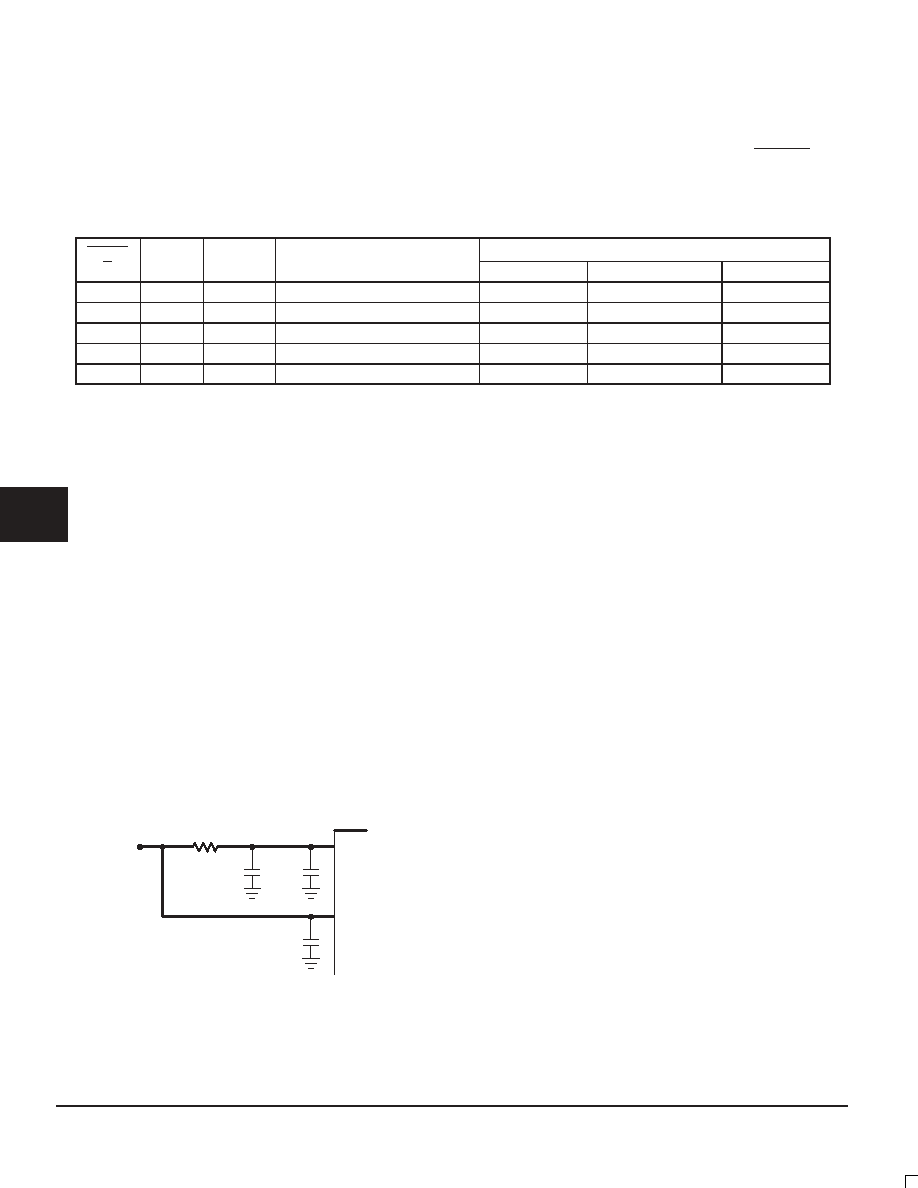
supply filter on the VCC_PLL pin for the MPC9653. Figure 3
illustrates a typical power supply filter scheme. The MPC9653
frequency and phase stability is most susceptible to noise with
spectral content in the 100kHz to 20MHz range. Therefore the
filter should be designed to target this range. The key parame-
ter that needs to be met in the final filter design is the DC volt-
age drop across the series filter resistor RF. From the data
sheet the ICCA current (the current sourced through the
VCC_PLL pin) is typically 5 mA (10 mA maximum), assuming
that a minimum of 2.985V must be maintained on the VCC_PLL
pin.
Figure 3. VCC_PLL Power Supply Filter
VCC_PLL
VCC
MPC9653
10 nF
RF = 5-15
CF
33...100 nF
RF
VCC
CF = 22 F
The minimum values for RF and the filter capacitor CF are
defined by the required filter characteristics: the RC filter
should provide an attenuation greater than 40 dB for noise
whose spectral content is above 100 kHz. In the example RC
filter shown in Figure 3 “VCC_PLL Power Supply Filter”, the filter
cut-off frequency is around 4 kHz and the noise attenuation at
100 kHz is better than 42 dB.
As the noise frequency crosses the series resonant point of
an individual capacitor its overall impedance begins to look
inductive and thus increases with increasing frequency. The
parallel capacitor combination shown ensures that a low im-
pedance path to ground exists for frequencies well above the
bandwidth of the PLL. Although the MPC9653 has several de-
sign features to minimize the susceptibility to power supply
noise (isolated power and grounds and fully differential PLL)
there still may be applications in which overall performance is
being degraded due to system power supply noise. The power
supply filter schemes discussed in this section should be ade-
quate to eliminate power supply noise related problems in
most designs.
Using the MPC9653 in zero–delay applications
Nested clock trees are typical applications for the
MPC9653. Designs using the MPC9653 as LVCMOS PLL fan-
out buffer with zero insertion delay will show significantly lower
clock skew than clock distributions developed from CMOS fan-
out buffers. The external feedback option of the MPC9653
clock driver allows for its use as a zero delay buffer. The PLL
aligns the feedback clock output edge with the clock input ref-
erence edge resulting a near zero delay through the device
(the propagation delay through the device is virtually elimi-
nated). The maximum insertion delay of the device in zero-
delay applications is measured between the reference clock
input and any output. This effective delay consists of the static
phase offset, I/O jitter (phase or long-term jitter), feedback path
delay and the output-to-output skew error relative to the feed-
back output.
相关PDF资料 |
PDF描述 |
|---|---|
| MPC9658ACR2 | 9658 SERIES, PLL BASED CLOCK DRIVER, 10 TRUE OUTPUT(S), 0 INVERTED OUTPUT(S), PQFP32 |
| MPC9658FA | 9658 SERIES, PLL BASED CLOCK DRIVER, 10 TRUE OUTPUT(S), 0 INVERTED OUTPUT(S), PQFP32 |
| MPC9658ACR2 | 9658 SERIES, PLL BASED CLOCK DRIVER, 10 TRUE OUTPUT(S), 0 INVERTED OUTPUT(S), PQFP32 |
| MPC973FA | 973 SERIES, PLL BASED CLOCK DRIVER, 12 TRUE OUTPUT(S), 0 INVERTED OUTPUT(S), PQFP52 |
| MPC974FAR2 | 974 SERIES, PLL BASED CLOCK DRIVER, 14 TRUE OUTPUT(S), 0 INVERTED OUTPUT(S), PQFP52 |
相关代理商/技术参数 |
参数描述 |
|---|---|
| MPC9658 | 制造商:MOTOROLA 制造商全称:Motorola, Inc 功能描述:3.3V 1:10 LVCMOS PLL Clock Generator |
| MPC9658AC | 功能描述:时钟发生器及支持产品 FSL 1-10 LVCMOS Zero Delay Buffer RoHS:否 制造商:Silicon Labs 类型:Clock Generators 最大输入频率:14.318 MHz 最大输出频率:166 MHz 输出端数量:16 占空比 - 最大:55 % 工作电源电压:3.3 V 工作电源电流:1 mA 最大工作温度:+ 85 C 安装风格:SMD/SMT 封装 / 箱体:QFN-56 |
| MPC9658ACR2 | 功能描述:时钟发生器及支持产品 FSL 1-10 LVCMOS Zero Delay Buffer RoHS:否 制造商:Silicon Labs 类型:Clock Generators 最大输入频率:14.318 MHz 最大输出频率:166 MHz 输出端数量:16 占空比 - 最大:55 % 工作电源电压:3.3 V 工作电源电流:1 mA 最大工作温度:+ 85 C 安装风格:SMD/SMT 封装 / 箱体:QFN-56 |
| MPC9658FA | 功能描述:时钟发生器及支持产品 2.5 3.3V 250MHz Clock Generator RoHS:否 制造商:Silicon Labs 类型:Clock Generators 最大输入频率:14.318 MHz 最大输出频率:166 MHz 输出端数量:16 占空比 - 最大:55 % 工作电源电压:3.3 V 工作电源电流:1 mA 最大工作温度:+ 85 C 安装风格:SMD/SMT 封装 / 箱体:QFN-56 |
| MPC9658FAR2 | 制造商:Integrated Device Technology Inc 功能描述:PLL Clock Driver Single 32-Pin LQFP T/R 制造商:Integrated Device Technology Inc 功能描述:MPC9658FAR2 - Tape and Reel |
发布紧急采购,3分钟左右您将得到回复。