- 您现在的位置:买卖IC网 > PDF目录385632 > MPS8599 (ON SEMICONDUCTOR) Amplifier Transistors Voltage and Current are Negative for PNP Transistors(放大器晶体管) PDF资料下载
参数资料
| 型号: | MPS8599 |
| 厂商: | ON SEMICONDUCTOR |
| 元件分类: | 功率晶体管 |
| 英文描述: | Amplifier Transistors Voltage and Current are Negative for PNP Transistors(放大器晶体管) |
| 中文描述: | 500 mA, 80 V, PNP, Si, SMALL SIGNAL TRANSISTOR, TO-92 |
| 封装: | CASE 29-11, TO-226, 3 PIN |
| 文件页数: | 1/7页 |
| 文件大小: | 82K |
| 代理商: | MPS8599 |
Semiconductor Components Industries, LLC, 2006
January, 2006 Rev. 5
1
Publication Order Number:
MPS8098/D
(NPN) MPS8098, MPS8099*,
(PNP) MPS8598, MPS8599*
*Preferred Devices
Amplifier Transistors
Voltage and Current are Negative
for PNP Transistors
Features
PbFree Packages are Available*
MAXIMUM RATINGS
Rating
Symbol
Value
Unit
CollectorEmitter Voltage
MPS8098, MPS8598
MPS8099, MPS8599
V
CEO
60
80
Vdc
CollectorBase Voltage
MPS8098, MPS8598
MPS8099, MPS8599
V
CBO
60
80
Vdc
EmitterBase Voltage
V
EBO
4.0
Vdc
Collector Current Continuous
I
C
500
mAdc
Total Device Dissipation @ T
A
= 25
°
C
Derate above 25
°
C
P
D
625
5.0
mW
mW/
°
C
Total Device Dissipation @ T
C
= 25
°
C
Derate above 25
°
C
P
D
1.5
12
W
mW/
°
C
Operating and Storage Junction
Temperature Range
T
J
, T
stg
55 to +150
°
C
THERMAL CHARACTERISTICS
Characteristic
Symbol
Max
Unit
Thermal Resistance, JunctiontoAmbient
(Note 1)
R
JA
200
°
C/W
Thermal Resistance, JunctiontoCase
R
JC
83.3
°
C/W
Maximum ratings are those values beyond which device damage can occur.
Maximum ratings applied to the device are individual stress limit values (not
normal operating conditions) and are not valid simultaneously. If these limits are
exceeded, device functional operation is not implied, damage may occur and
reliability may be affected.
1. R
JA
is measured with the device soldered into a typical printed circuit board.
*For additional information on our PbFree strategy and soldering details, please
download the ON Semiconductor Soldering and Mounting Techniques
Reference Manual, SOLDERRM/D.
Preferred
devices are recommended choices for future use
and best overall value.
http://onsemi.com
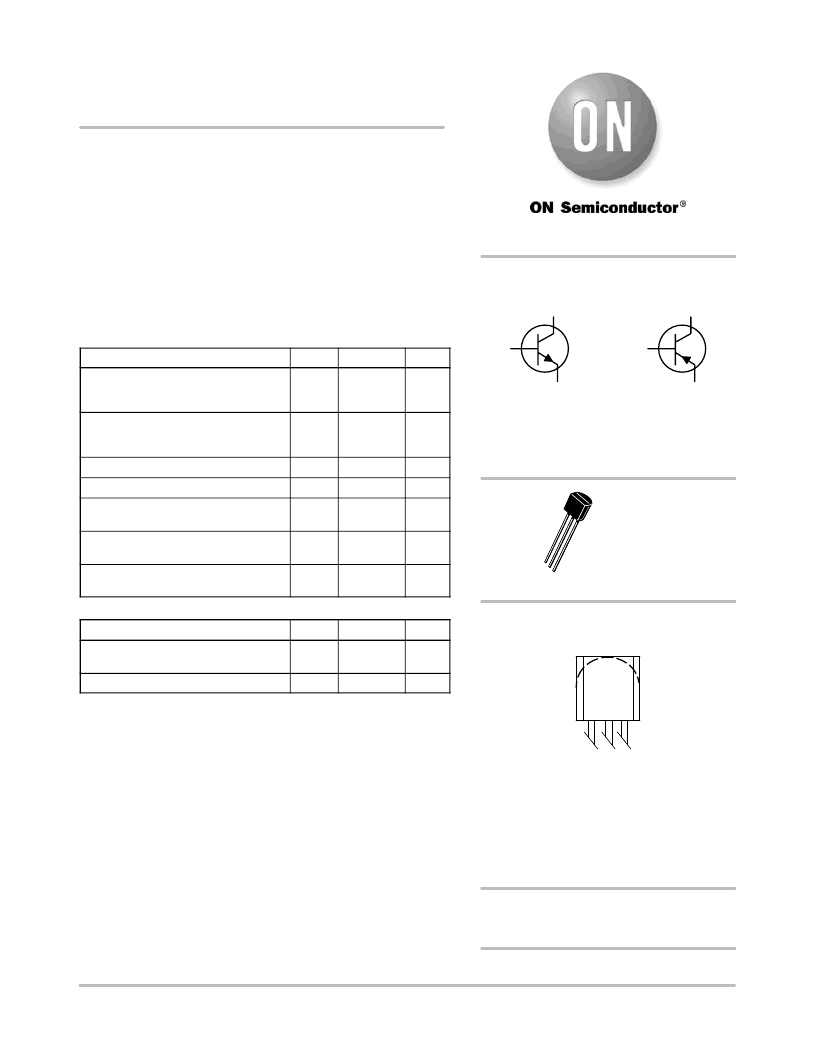
COLLECTOR
3
2
BASE
1
EMITTER
STYLE 1
MPS8098,
MPS8099
NPN
COLLECTOR
3
2
BASE
1
EMITTER
STYLE 1
MPS8598,
MPS8599
PNP
See detailed ordering and shipping information in the package
dimensions section on page 6 of this data sheet.
ORDERING INFORMATION
MPS8x9y = Device Code
x = 0 or 5
y = 8 or 9
= Assembly Location
= Year
= Work Week
= PbFree Package
A
Y
WW
(Note: Microdot may be in either location)
TO92
CASE 2911
STYLE 1
1
23
MARKING DIAGRAM
MPS
8x9y
AYWW
相关PDF资料 |
PDF描述 |
|---|---|
| MPSA05 | Amplifier Transistors Voltage and Current are Negative for PNP Transistors(放大器晶体管) |
| MPSA06 | Amplifier Transistors Voltage and Current are Negative for PNP Transistors(NPN通用放大器) |
| MPSA18 | Low Noise Transistor NPN Silicon(NPN低噪声晶体管) |
| MPSA29 | Darlington Transistors NPN Silicon(NPN达林顿晶体管) |
| MPSA42 | High Voltage Transistors NPN Silicon(NPN高电压放大器) |
相关代理商/技术参数 |
参数描述 |
|---|---|
| MPS8599G | 功能描述:两极晶体管 - BJT 500mA 80V PNP RoHS:否 制造商:STMicroelectronics 配置: 晶体管极性:PNP 集电极—基极电压 VCBO: 集电极—发射极最大电压 VCEO:- 40 V 发射极 - 基极电压 VEBO:- 6 V 集电极—射极饱和电压: 最大直流电集电极电流: 增益带宽产品fT: 直流集电极/Base Gain hfe Min:100 A 最大工作温度: 安装风格:SMD/SMT 封装 / 箱体:PowerFLAT 2 x 2 |
| MPS8599RLRA | 功能描述:两极晶体管 - BJT 500mA 80V PNP RoHS:否 制造商:STMicroelectronics 配置: 晶体管极性:PNP 集电极—基极电压 VCBO: 集电极—发射极最大电压 VCEO:- 40 V 发射极 - 基极电压 VEBO:- 6 V 集电极—射极饱和电压: 最大直流电集电极电流: 增益带宽产品fT: 直流集电极/Base Gain hfe Min:100 A 最大工作温度: 安装风格:SMD/SMT 封装 / 箱体:PowerFLAT 2 x 2 |
| MPS8599RLRAG | 功能描述:两极晶体管 - BJT 500mA 80V PNP RoHS:否 制造商:STMicroelectronics 配置: 晶体管极性:PNP 集电极—基极电压 VCBO: 集电极—发射极最大电压 VCEO:- 40 V 发射极 - 基极电压 VEBO:- 6 V 集电极—射极饱和电压: 最大直流电集电极电流: 增益带宽产品fT: 直流集电极/Base Gain hfe Min:100 A 最大工作温度: 安装风格:SMD/SMT 封装 / 箱体:PowerFLAT 2 x 2 |
| MPS8599RLRM | 制造商:ONSEMI 制造商全称:ON Semiconductor 功能描述:Amplifier Transistors Voltage and Current are Negative for PNP Transistors |
| MPS8599RLRMG | 功能描述:两极晶体管 - BJT 500mA 80V PNP RoHS:否 制造商:STMicroelectronics 配置: 晶体管极性:PNP 集电极—基极电压 VCBO: 集电极—发射极最大电压 VCEO:- 40 V 发射极 - 基极电压 VEBO:- 6 V 集电极—射极饱和电压: 最大直流电集电极电流: 增益带宽产品fT: 直流集电极/Base Gain hfe Min:100 A 最大工作温度: 安装风格:SMD/SMT 封装 / 箱体:PowerFLAT 2 x 2 |
发布紧急采购,3分钟左右您将得到回复。