- 您现在的位置:买卖IC网 > Datasheet目录345 > MT42L256M32D4KP-3 IT:A (Micron Technology Inc)IC LPDDR2 SDRAM 8GBIT 168FBGA Datasheet资料下载
参数资料
| 型号: | MT42L256M32D4KP-3 IT:A |
| 厂商: | Micron Technology Inc |
| 文件页数: | 65/164页 |
| 文件大小: | 0K |
| 描述: | IC LPDDR2 SDRAM 8GBIT 168FBGA |
| 标准包装: | 1,000 |
| 格式 - 存储器: | RAM |
| 存储器类型: | 移动 LPDDR2 SDRAM |
| 存储容量: | 8G(356M x 32) |
| 速度: | 333MHz |
| 接口: | 并联 |
| 电源电压: | 1.14 V ~ 1.3 V |
| 工作温度: | -25°C ~ 85°C |
| 封装/外壳: | 168-VFBGA |
| 供应商设备封装: | 168-FBGA(12x12) |
| 包装: | 散装 |
第1页第2页第3页第4页第5页第6页第7页第8页第9页第10页第11页第12页第13页第14页第15页第16页第17页第18页第19页第20页第21页第22页第23页第24页第25页第26页第27页第28页第29页第30页第31页第32页第33页第34页第35页第36页第37页第38页第39页第40页第41页第42页第43页第44页第45页第46页第47页第48页第49页第50页第51页第52页第53页第54页第55页第56页第57页第58页第59页第60页第61页第62页第63页第64页当前第65页第66页第67页第68页第69页第70页第71页第72页第73页第74页第75页第76页第77页第78页第79页第80页第81页第82页第83页第84页第85页第86页第87页第88页第89页第90页第91页第92页第93页第94页第95页第96页第97页第98页第99页第100页第101页第102页第103页第104页第105页第106页第107页第108页第109页第110页第111页第112页第113页第114页第115页第116页第117页第118页第119页第120页第121页第122页第123页第124页第125页第126页第127页第128页第129页第130页第131页第132页第133页第134页第135页第136页第137页第138页第139页第140页第141页第142页第143页第144页第145页第146页第147页第148页第149页第150页第151页第152页第153页第154页第155页第156页第157页第158页第159页第160页第161页第162页第163页第164页
�� �
�
�2Gb:� x16,� x32� Mobile� LPDDR2� SDRAM� S4�
�BURST� TERMINATE� Command�
�WRITEs� Interrupted� by� a� WRITE�
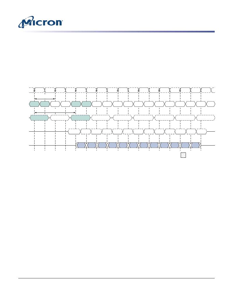
�A� burst� WRITE� can� only� be� interrupted� by� another� WRITE� with� a� 4-bit� burst� boundary,�
�provided� that� t� CCD� (MIN)� is� met.�
�A� WRITE� burst� interrupt� can� occur� on� even� clock� cycles� after� the� initial� WRITE� com-�
�mand,� provided� that� t� CCD� (MIN)� is� met.�
�Figure� 43:� WRITE� Burst� Interrupt� Timing� –� WL� =� 1,� BL� =� 8,� t� CCD� =� 2�
�T0�
�T1�
�T2�
�T3�
�T4�
�T5�
�T6�
�T7�
�T8�
�CK#�
�CK�
�WL� =� 1�
�CA[9:0]�
�Bank� m�
�col� addr� a�
�Col� addr� a�
�Bank� n�
�col� addr� b�
�Col� addr� b�
�t� CCD�
�=2�
�CMD�
�WRITE�
�NOP�
�WRITE�
�NOP�
�NOP�
�NOP�
�NOP�
�NOP�
�NOP�
�DQS#�
�DQS�
�DQ�
�D� IN� A0�
�D� IN� A1�
�D� IN� A2�
�D� IN� A3�
�D� IN� B0�
�D� IN� B1�
�D� IN� B2�
�D� IN� B3�
�D� IN� B4�
�D� IN� B5�
�D� IN� B6�
�D� IN� B7�
�Transitioning� data�
�Notes:�
�1.� WRITEs� can� only� be� interrupted� by� other� WRITEs� or� the� BST� command.�
�2.� The� effective� burst� length� of� the� first� WRITE� equals� two� times� the� number� of� clock� cycles�
�between� the� first� WRITE� and� the� interrupting� WRITE.�
�BURST� TERMINATE� Command�
�The� BURST� TERMINATE� (BST)� command� is� initiated� with� CS#� LOW,� CA0� HIGH,� CA1�
�HIGH,� CA2� LOW,� and� CA3� LOW� at� the� rising� edge� of� the� clock.� A� BST� command� can� only�
�be� issued� to� terminate� an� active� READ� or� WRITE� burst.� Therefore,� a� BST� command� can�
�only� be� issued� up� to� and� including� BL/2� -� 1� clock� cycles� after� a� READ� or� WRITE� com-�
�mand.� The� effective� burst� length� of� a� READ� or� WRITE� command� truncated� by� a� BST�
�command� is� as� follows:�
�?� Effective� burst� length� =� 2� � (number� of� clock� cycles� from� the� READ� or� WRITE� com-�
�mand� to� the� BST� command).�
�?� If� a� READ� or� WRITE� burst� is� truncated� with� a� BST� command,� the� effective� burst� length�
�of� the� truncated� burst� should� be� used� for� BL� when� calculating� the� minimum� READ-�
�to-WRITE� or� WRITE-to-READ� delay.�
�?� The� BST� command� only� affects� the� most� recent� READ� or� WRITE� command.� The� BST�
�command� truncates� an� ongoing� READ� burst� RL� � t� CK� +� t� DQSCK� +� t� DQSQ� after� the� ris-�
�ing� edge� of� the� clock� where� the� BST� command� is� issued.� The� BST� command� truncates�
�an� ongoing� WRITE� burst� WL� � t� CK� +� t� DQSS� after� the� rising� edge� of� the� clock� where� the�
�BST� command� is� issued.�
�PDF:� 09005aef83f3f2eb�
�2gb_mobile_lpddr2_s4_g69a.pdf� –� Rev.� N� 3/12� EN�
�65�
�Micron� Technology,� Inc.� reserves� the� right� to� change� products� or� specifications� without� notice.�
�2010� Micron� Technology,� Inc.� All� rights� reserved.�
�相关PDF资料 |
PDF描述 |
|---|---|
| MT45W1MW16BDGB-708 AT | IC PSRAM 16MBIT 104MHZ 54VFBGA |
| MT48H32M16LFB4-75B IT:C | IC SDRAM 512MB 54VFBGA |
| MT48H8M16LFB4-75 IT:K TR | IC SDRAM 128MBIT 133MHZ 54VFBGA |
| MTC100-JA2-P34 | CONTACT INSERT PIN |
| MX841BE | IC CONVERTER WHITE LED 8-SOIC |
相关代理商/技术参数 |
参数描述 |
|---|---|
| MT42L256M32D4KP-MS | 制造商:Micron Technology Inc 功能描述:256MX32 LPDDR2 PLASTIC IND TEMP GREEN WFBGA 1.2V - Bulk |
发布紧急采购,3分钟左右您将得到回复。