- 您现在的位置:买卖IC网 > PDF目录187166 > MT48LC8M16LFTG-10XT:G 8M X 16 SYNCHRONOUS DRAM, 7 ns, PDSO54 PDF资料下载
参数资料
| 型号: | MT48LC8M16LFTG-10XT:G |
| 元件分类: | DRAM |
| 英文描述: | 8M X 16 SYNCHRONOUS DRAM, 7 ns, PDSO54 |
| 封装: | 0.400 INCH, PLASTIC, TSOP2-54 |
| 文件页数: | 1/79页 |
| 文件大小: | 2760K |
当前第1页第2页第3页第4页第5页第6页第7页第8页第9页第10页第11页第12页第13页第14页第15页第16页第17页第18页第19页第20页第21页第22页第23页第24页第25页第26页第27页第28页第29页第30页第31页第32页第33页第34页第35页第36页第37页第38页第39页第40页第41页第42页第43页第44页第45页第46页第47页第48页第49页第50页第51页第52页第53页第54页第55页第56页第57页第58页第59页第60页第61页第62页第63页第64页第65页第66页第67页第68页第69页第70页第71页第72页第73页第74页第75页第76页第77页第78页第79页
Products and specifications discussed herein are subject to change by Micron without notice.
128Mb: x16, x32 Mobile SDRAM
Features
PDF: 09005aef807f4885/Source: 09005aef8071a76b
Micron Technology, Inc., reserves the right to change products or specifications without notice.
128Mbx16x32Mobile_1.fm - Rev. L 10/07 EN
1
2001 Micron Technology, Inc. All rights reserved.
Mobile SDRAM
MT48LC8M16LF, MT48V8M16LF, MT48LC4M32LF, MT48V4M32LF
Features
Temperature-compensated self refresh (TCSR)
Fully synchronous; all signals registered on positive
edge of system clock
Internal pipelined operation; column address can be
changed every clock cycle
Internal banks for hiding row access/precharge
Programmable burst lengths: 1, 2, 4, 8, or full page
Auto precharge, includes concurrent auto precharge,
and auto refresh modes
Self refresh mode; standard and low power
64ms, 4,096-cycle refresh (15.6s/row)
LVTTL-compatible inputs and outputs
Low voltage power supply
Partial-array self refresh (PASR) power-saving mode
Notes: 1. x16 only.
2. x32 only.
3. Contact Micron for availability.
Options
Mark
VDD/VDDQ
– 3.3V/3.3V
LC
– 2.5V/2.5–1.8V
V
Configurations
– 8 Meg x 16 (2 Meg x 16 x 4 banks)
8M16
– 4 Meg x 32 (1 Meg x 32 x 4 banks)
4M32
Package/ball out
– 54-ball VFBGA (8mm x 8mm)1
F4
– 54-ball VFBGA (8mm x 8mm)1 Pb-free
B4
– 90-ball VFBGA (8mm x 13mm)2
F5
– 90-ball VFBGA (8mm x 13mm)2 Pb-free
B5
– 54-pin TSOP II (400 mil)
TG3
– 54-pin TSOP II (400 mil) Pb-free
P3
Timing (cycle time)
– 7.5ns @ CL = 3 (133 MHz)
-75M3
– 8ns @ CL = 3 (125 MHz)
-8
– 10ns @ CL = 3 (100 MHz)
Temperature
– Commercial (0°C to +70°C)
None
– Industrial (–40°C to +85°C)
IT
– Extended (–25°C to +75°C)
XT3
Design revision
:G
Part Number Example:
MT48V8M16LFB4-8:G
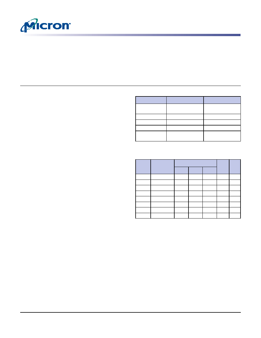
Table 1:
Configurations
8 Meg x 16
4 Meg x 32
Configuration
2 Meg x 16 x 4
banks
1 Meg x 32 x 4
banks
Refresh count
4K
Row addressing
4K (A0–A11)
Bank addressing
4 (BA0, BA1)
Column
addressing
512 (A0–A8)
256 (A0–A7)
Table 2:
Key Timing Parameters
CL = CAS (READ) latency
Speed
Grade
Clock
Frequency
Access Time
tRCD tRP
CL = 1 CL = 2 CL = 3
-75M
133 MHz
–
5.4
19ns
-8
125 MHz
–
7ns
20ns
-10
100 MHz
–
7ns
20ns
-75M
100 MHz
–
6
–
19ns
-8
100 MHz
–
8ns
–
20ns
-10
83 MHz
–
8ns
–
20ns
-8
50 MHz
19ns
–
20ns
-10
40 MHz
22ns
–
20ns
相关PDF资料 |
PDF描述 |
|---|---|
| MT4C1024DJ-6IT | 1M X 1 FAST PAGE DRAM, 60 ns, PDSO20 |
| MT4LSD232UG-10C1 | 2M X 32 SYNCHRONOUS DRAM MODULE, 7.5 ns, SMA100 |
| MT4S06 | UHF BAND, Si, NPN, RF SMALL SIGNAL TRANSISTOR |
| MT4S104T | UHF BAND, SiGe, NPN, RF SMALL SIGNAL TRANSISTOR |
| MT4S104U | KA BAND, SiGe, NPN, RF SMALL SIGNAL TRANSISTOR |
相关代理商/技术参数 |
参数描述 |
|---|---|
| MT48LC8M32B2 | 制造商:MICRON 制造商全称:Micron Technology 功能描述:SYNCHRONOUS DRAM |
发布紧急采购,3分钟左右您将得到回复。