- 您现在的位置:买卖IC网 > PDF目录98045 > MTB60N05HD (ON SEMICONDUCTOR) 60 A, 50 V, 0.014 ohm, N-CHANNEL, Si, POWER, MOSFET PDF资料下载
参数资料
| 型号: | MTB60N05HD |
| 厂商: | ON SEMICONDUCTOR |
| 元件分类: | JFETs |
| 英文描述: | 60 A, 50 V, 0.014 ohm, N-CHANNEL, Si, POWER, MOSFET |
| 封装: | D2PAK-3 |
| 文件页数: | 9/13页 |
| 文件大小: | 161K |
| 代理商: | MTB60N05HD |
MTB60N05HDL
http://onsemi.com
5
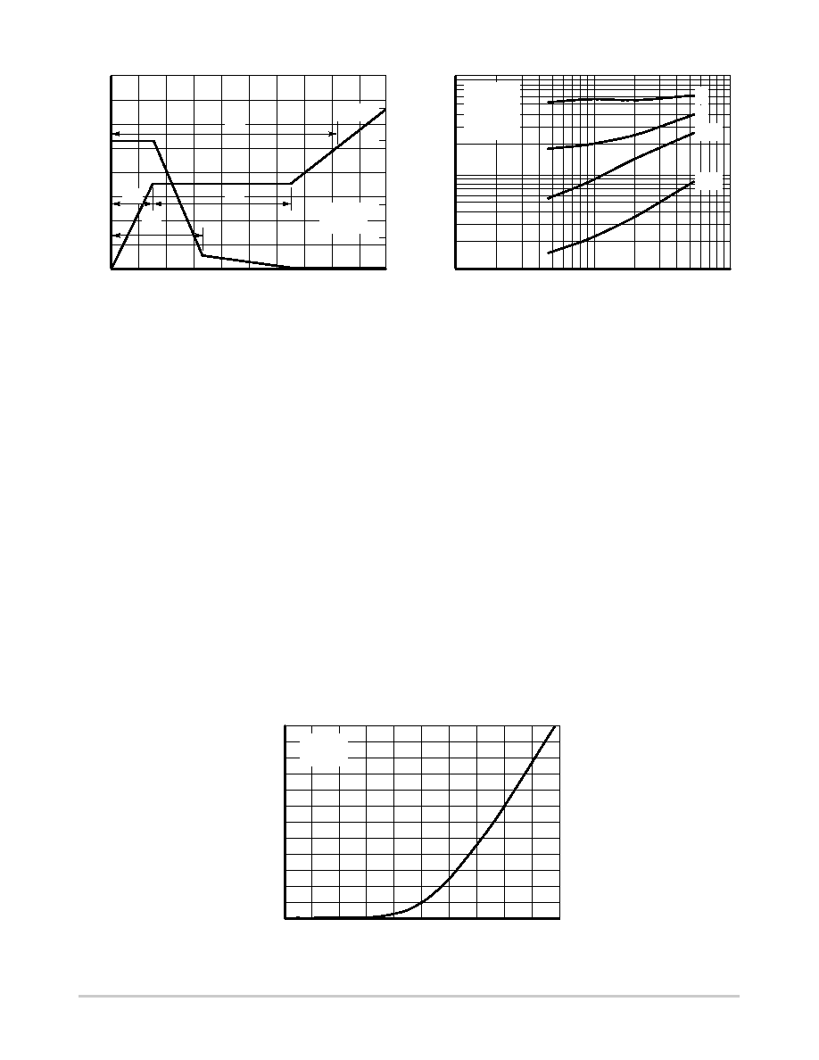
Figure 8. Gate–To–Source and Drain–To–Source
Voltage versus Total Charge
Figure 9. Resistive Switching Time
Variation versus Gate Resistance
QG, TOTAL GATE CHARGE (nC)
RG, GATE RESISTANCE (OHMS)
t,TIME
(ns)
V DS
,DRAIN-T
O-SOURCE
VOL
TAGE
(VOL
TS)
V GS
,GA
TE-T
O-SOURCE
VOL
TAGE
(VOL
TS)
1.0
10
100
10
100
1000
VDD = 25 V
ID = 60 A
VGS = 5.0 V
TJ = 25°C
010
40
50
20
30
6.0
2.0
0
8.0
4.0
60
50
40
30
10
20
0
TJ = 60°C
ID = 5.0 A
Q2
Q1
QT
Q3
VDS
VGS
tr
tf
td(off)
td(on)
DRAIN–TO–SOURCE DIODE CHARACTERISTICS
The switching characteristics of a MOSFET body diode
are very important in systems using it as a freewheeling or
commutating diode. Of particular interest are the reverse
recovery characteristics which play a major role in
determining switching losses, radiated noise, EMI and RFI.
System switching losses are largely due to the nature of
the body diode itself. The body diode is a minority carrier
device, therefore it has a finite reverse recovery time, trr, due
to the storage of minority carrier charge, QRR, as shown in
the typical reverse recovery wave form of Figure 11. It is this
stored charge that, when cleared from the diode, passes
through a potential and defines an energy loss. Obviously,
repeatedly forcing the diode through reverse recovery
further increases switching losses. Therefore, one would
like a diode with short trr and low QRR specifications to
minimize these losses.
The abruptness of diode reverse recovery effects the
amount of radiated noise, voltage spikes, and current
ringing. The mechanisms at work are finite irremovable
circuit parasitic inductances and capacitances acted upon by
high di/dts. The diode’s negative di/dt during ta is directly
controlled by the device clearing the stored charge.
However, the positive di/dt during tb is an uncontrollable
diode characteristic and is usually the culprit that induces
current ringing. Therefore, when comparing diodes, the
ratio of tb/ta serves as a good indicator of recovery
abruptness and thus gives a comparative estimate of
probable noise generated. A ratio of 1 is considered ideal and
values less than 0.5 are considered snappy.
Compared to ON Semiconductor standard cell density
low voltage MOSFETs, high cell density MOSFET diodes
are faster (shorter trr), have less stored charge and a softer
reverse recovery characteristic. The softness advantage of
the high cell density diode means they can be forced through
reverse recovery at a higher di/dt than a standard cell
MOSFET diode without increasing the current ringing or the
noise generated. In addition, power dissipation incurred
from switching the diode will be less due to the shorter
recovery time and lower switching losses.
Figure 10. Diode Forward Voltage versus Current
I S
,SOURCE
CURRENT
(AMPS)
VSD, SOURCE-TO-DRAIN VOLTAGE (VOLTS)
0
10
30
50
60
40
20
0.5
0.6
0.7
0.8
0.9
1.0
VGS = 0 V
TJ = 25°C
相关PDF资料 |
PDF描述 |
|---|---|
| MTB60N05HDL | 60 A, 50 V, 0.014 ohm, N-CHANNEL, Si, POWER, MOSFET |
| MTB60N05HDG | 60 A, 50 V, 0.014 ohm, N-CHANNEL, Si, POWER, MOSFET |
| MTB60N05HDLT4 | 60 A, 50 V, 0.014 ohm, N-CHANNEL, Si, POWER, MOSFET |
| MTB60N06HDT4 | 60 A, 60 V, 0.014 ohm, N-CHANNEL, Si, POWER, MOSFET |
| MTB60N06HD | 60 A, 60 V, 0.014 ohm, N-CHANNEL, Si, POWER, MOSFET |
相关代理商/技术参数 |
参数描述 |
|---|---|
| MTB60N05HDL | 制造商:Motorola Inc 功能描述: 制造商:ON Semiconductor 功能描述: 制造商:MOTOROLA 功能描述: |
| MTB60N05HDLT4 | 制造商:Rochester Electronics LLC 功能描述:- Bulk |
| MTB60N06 | 制造商:MOTOROLA 制造商全称:Motorola, Inc 功能描述:TMOS POWER FET 60 AMPERES 60 VOLTS |
| MTB60N06HD | 制造商:ON Semiconductor 功能描述:Trans MOSFET N-CH 60V 60A 3-Pin(2+Tab) D2PAK |
| MTB60N06HDT4 | 制造商:ON Semiconductor 功能描述:Trans MOSFET N-CH 60V 60A 3-Pin(2+Tab) D2PAK T/R 制造商:Rochester Electronics LLC 功能描述:- Bulk |
发布紧急采购,3分钟左右您将得到回复。