- 您现在的位置:买卖IC网 > PDF目录98048 > MTP29N15E (ON SEMICONDUCTOR) 29 A, 150 V, 0.07 ohm, N-CHANNEL, Si, POWER, MOSFET, TO-220AB PDF资料下载
参数资料
| 型号: | MTP29N15E |
| 厂商: | ON SEMICONDUCTOR |
| 元件分类: | JFETs |
| 英文描述: | 29 A, 150 V, 0.07 ohm, N-CHANNEL, Si, POWER, MOSFET, TO-220AB |
| 封装: | CASE 221A-09, 3 PIN |
| 文件页数: | 9/12页 |
| 文件大小: | 115K |
| 代理商: | MTP29N15E |
MTP29N15E
http://onsemi.com
6
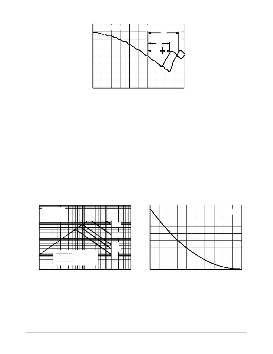
I S
,SOURCE
CURRENT
t, TIME
Figure 11. Reverse Recovery Time (trr)
di/dt = 300 A/s
Standard Cell Density
High Cell Density
tb
trr
ta
trr
SAFE OPERATING AREA
The Forward Biased Safe Operating Area curves define
the maximum simultaneous drain–to–source voltage and
drain current that a transistor can handle safely when it is
forward biased. Curves are based upon maximum peak
junction temperature and a case temperature (TC) of 25°C.
Peak repetitive pulsed power limits are determined by using
the thermal response data in conjunction with the procedures
discussed in AN569, “Transient Thermal Resistance –
General Data and Its Use.”
Switching between the off–state and the on–state may
traverse any load line provided neither rated peak current
(IDM) nor rated voltage (VDSS) is exceeded, and that the
transition time (tr, tf) does not exceed 10 s. In addition the
total power averaged over a complete switching cycle must
not exceed (TJ(MAX) – TC)/(R
θJC).
A power MOSFET designated E–FET can be safely used
in switching circuits with unclamped inductive loads. For
reliable operation, the stored energy from circuit inductance
dissipated in the transistor while in avalanche must be less
than the rated limit and must be adjusted for operating
conditions differing from those specified. Although industry
practice is to rate in terms of energy, avalanche energy
capability is not a constant. The energy rating decreases
non–linearly with an increase of peak current in avalanche
and peak junction temperature.
Figure 12. Maximum Rated Forward Biased
Safe Operating Area
0.1
VDS, DRAIN-TO-SOURCE VOLTAGE (VOLTS)
1
I D
,DRAIN
CURRENT
(AMPS)
RDS(on) LIMIT
THERMAL LIMIT
PACKAGE LIMIT
10
0.1
dc
1
1000
Figure 13. Maximum Avalanche Energy versus
Starting Junction Temperature
25
TJ, STARTING JUNCTION TEMPERATURE (°C)
100
200
E AS
,SINGLE
PULSE
DRAIN-T
O-SOURCE
75
0
50
150
100
125
300
400
AV
ALANCHE
ENERGY
(mJ)
10
10 ms
1 ms
100 ms
ID = 29 A
50
150
450
250
350
10 ms
VGS = 20 V
SINGLE PULSE
TC = 25°C
100
相关PDF资料 |
PDF描述 |
|---|---|
| MTSF1P02HDR2 | 1800 mA, 20 V, P-CHANNEL, Si, SMALL SIGNAL, MOSFET |
| MTSF1P02HDR2 | 1800 mA, 20 V, P-CHANNEL, Si, SMALL SIGNAL, MOSFET |
| MTSF2P02HDR2 | 3000 mA, 20 V, P-CHANNEL, Si, SMALL SIGNAL, MOSFET |
| MTSF2P02HDR2 | 2400 mA, 20 V, P-CHANNEL, Si, SMALL SIGNAL, MOSFET |
| MTSF2P03HDR2 | 2700 mA, 30 V, P-CHANNEL, Si, SMALL SIGNAL, MOSFET |
相关代理商/技术参数 |
参数描述 |
|---|---|
| MTP2H-E10-C | 功能描述:电缆束带 Mutiple Tie Plate, 2 Bundle, M-H Ties, # RoHS:否 制造商:Phoenix Contact 产品:Cable Tie Mounts 类型:Adhesive 颜色:Black 材料:Acrylonitrile Butadiene Styrene (ABS) 长度:19 mm 宽度:19 mm 抗拉强度: |
| MTP2H-E10-C39 | 功能描述:电缆束带 Mutiple Tie Plate, 2 Bundle, M-H Ties, # RoHS:否 制造商:Phoenix Contact 产品:Cable Tie Mounts 类型:Adhesive 颜色:Black 材料:Acrylonitrile Butadiene Styrene (ABS) 长度:19 mm 宽度:19 mm 抗拉强度: |
| MTP2H-E6-C | 功能描述:电缆束带 Mutiple Tie Plate, 2 Bundle, M-H Ties, # RoHS:否 制造商:Phoenix Contact 产品:Cable Tie Mounts 类型:Adhesive 颜色:Black 材料:Acrylonitrile Butadiene Styrene (ABS) 长度:19 mm 宽度:19 mm 抗拉强度: |
| MTP2N20 | 制造商:MOTOROLA 制造商全称:Motorola, Inc 功能描述:POWER FIELD EFFECT TRANSISTOR, N-CHANNEL ENHANCEMENT-MODE SILICON GATE |
| MTP2N35 | 制造商:FAIRCHILD 制造商全称:Fairchild Semiconductor 功能描述:N-Channel Power MOSFETs, 2.25A, 350-400V |
发布紧急采购,3分钟左右您将得到回复。