- 您现在的位置:买卖IC网 > PDF目录9924 > MX7575JEWN+T (Maxim Integrated Products)IC ADC 8BIT MPU COMP 18-SOIC PDF资料下载
参数资料
| 型号: | MX7575JEWN+T |
| 厂商: | Maxim Integrated Products |
| 文件页数: | 11/12页 |
| 文件大小: | 0K |
| 描述: | IC ADC 8BIT MPU COMP 18-SOIC |
| 产品培训模块: | Lead (SnPb) Finish for COTS Obsolescence Mitigation Program |
| 标准包装: | 1,000 |
| 位数: | 8 |
| 采样率(每秒): | 200k |
| 数据接口: | 并联 |
| 转换器数目: | 1 |
| 功率耗散(最大): | 762mW |
| 电压电源: | 单电源 |
| 工作温度: | -40°C ~ 85°C |
| 安装类型: | 表面贴装 |
| 封装/外壳: | 18-SOIC(0.295",7.50mm 宽) |
| 供应商设备封装: | 18-SOIC W |
| 包装: | 带卷 (TR) |
| 输入数目和类型: | 1 个单端,单极 |
MX7575/MX7576
MX7575 Track/Hold
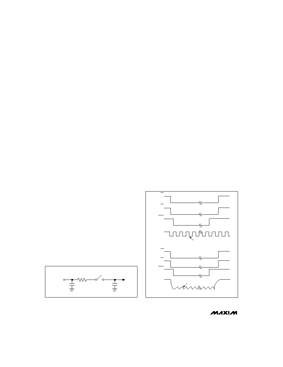
The track/hold consists of a sampling capacitor and a
switch to capture the input signal. The simplified dia-
gram of this block is shown in Figure 11. At the begin-
ning of the conversion, switch S1 is closed, and the
input signal is tracked. The input signal is held (switch
S1 opens) on the third falling edge of clock after
CS
and
RD go low (Figure 12). This allows a minimum of
two clock cycles for the input capacitor to be charged
to the input voltage through the switch resistance. The
time required for the hold capacitor to settle to ±1/4LSB
is typically 7ns. Therefore, the input signal is allowed
ample time to settle before it is acquired by the
track/hold. When a conversion ends, switch S1 closes,
and the input signal is tracked.
The track/hold is capable of acquiring signals with slew
rates of up to 386mV/s (or equivalently a 50kHz sine
wave with 2.46Vp-p amplitude). Figure 13 shows the
signal-to-noise ratio (SNR) versus input frequency for
the ADC. The SNR plot is generated at a sampling rate
of 200kHz using sinusoidal inputs with a peak-to-peak
amplitude of 2.46V. The reconstructed sine wave is
passed through a 50kHz 8th-order Chebychev filter.
The improvement in SNR at high frequencies is due to
the filter cutoff.
The switching nature of the analog input results in tran-
sient currents that charge the input capacitance of the
track/hold. Keep the driving source impedance low
(below 2k
), so that the settling characteristics of the
track/hold are not degraded. A low driving impedance
also minimizes undesirable noise pickup and reduces
DC errors caused by transient currents at the analog
input. As with any ADC, it is important to keep external
sources of noise to a minimum during a conversion.
Therefore, keep the data bus as quiet as possible dur-
ing a conversion, especially when the track/hold is
making the transition to the hold mode.
For conversion times that are significantly longer than
5s, the device’s accuracy may degrade slightly, as
shown in Figure 14. This degradation is due to the
charge that is lost from the hold capacitor in the pres-
ence of small on-chip leakage currents.
MX7576 Analog Input
The MX7576 analog input can also be modeled with the
switch and capacitor as shown in Figure 11. However,
unlike the MX7575, the MX7576 samples the input volt-
age eight times during a conversion (once before each
comparator decision). Therefore, the precautions that
apply to the MX7575 also apply to the MX7576. These
include minimizing the analog source impedance and
reducing noise coupling from the digital circuitry during
a conversion, especially near a sampling instant.
Reference Input
The high speed of this ADC can be partially attributed to
the “inverted voltage output” topology of the DAC that it
uses. This topology provides low offset and gain errors
and fast settling times. The input current to the DAC,
however, is not constant. During a conversion, as differ-
ent DAC codes are tried, the DC impedance of the DAC
can vary between 6k
and 18k. Furthermore, when
the DAC codes change, small amounts of transient cur-
rent are drawn from the reference input. These charac-
teristics require a low DC and AC driving impedance for
the reference circuitry to minimize conversion errors.
Figure 15 shows the reference circuitry recommended
to drive the reference input of the MX7575/MX7576.
CMOS, P-Compatible, 5s/10s, 8-Bit ADCs
8
_______________________________________________________________________________________
VIN
CS
0.5pF
CH
2pF
RON
500
S1
Figure 11. Equivalent Input Circuit
CS
RD
BUSY
INTERNAL
CLOCK
CS
RD
BUSY
EXTERNAL
CLOCK
INPUT SIGNAL HELD HERE
a) WITH EXTERNAL CLOCK
b) WITH INTERNAL CLOCK
INPUT SIGNAL HELD HERE
Figure 12. MX7575 Track/Hold (Slow-Memory Interface)
Timing Diagrams
相关PDF资料 |
PDF描述 |
|---|---|
| MS27473E10F5PA | CONN PLUG 5POS STRAIGHT W/PINS |
| ICL3232ECV-16Z-T7A | IC TXRX RS232 DUAL ESD 16TSSOP |
| IDT723673L15PF | IC FIFO SYNC 8192X36 128QFP |
| MX7576KP+T | IC ADC 8BIT MPU COMP 20-PLCC |
| IDT72V293L7-5PF8 | IC FIFO 65536X18 7-5NS 80QFP |
相关代理商/技术参数 |
参数描述 |
|---|---|
| MX7575JN | 功能描述:模数转换器 - ADC RoHS:否 制造商:Texas Instruments 通道数量:2 结构:Sigma-Delta 转换速率:125 SPs to 8 KSPs 分辨率:24 bit 输入类型:Differential 信噪比:107 dB 接口类型:SPI 工作电源电压:1.7 V to 3.6 V, 2.7 V to 5.25 V 最大工作温度:+ 85 C 安装风格:SMD/SMT 封装 / 箱体:VQFN-32 |
| MX7575JN+ | 功能描述:模数转换器 - ADC 8-Bit Precision DAC RoHS:否 制造商:Texas Instruments 通道数量:2 结构:Sigma-Delta 转换速率:125 SPs to 8 KSPs 分辨率:24 bit 输入类型:Differential 信噪比:107 dB 接口类型:SPI 工作电源电压:1.7 V to 3.6 V, 2.7 V to 5.25 V 最大工作温度:+ 85 C 安装风格:SMD/SMT 封装 / 箱体:VQFN-32 |
| MX7575JP | 功能描述:模数转换器 - ADC RoHS:否 制造商:Texas Instruments 通道数量:2 结构:Sigma-Delta 转换速率:125 SPs to 8 KSPs 分辨率:24 bit 输入类型:Differential 信噪比:107 dB 接口类型:SPI 工作电源电压:1.7 V to 3.6 V, 2.7 V to 5.25 V 最大工作温度:+ 85 C 安装风格:SMD/SMT 封装 / 箱体:VQFN-32 |
| MX7575JP+ | 功能描述:模数转换器 - ADC 8-Bit Precision DAC RoHS:否 制造商:Texas Instruments 通道数量:2 结构:Sigma-Delta 转换速率:125 SPs to 8 KSPs 分辨率:24 bit 输入类型:Differential 信噪比:107 dB 接口类型:SPI 工作电源电压:1.7 V to 3.6 V, 2.7 V to 5.25 V 最大工作温度:+ 85 C 安装风格:SMD/SMT 封装 / 箱体:VQFN-32 |
| MX7575JP+T | 功能描述:模数转换器 - ADC 8-Bit Precision DAC RoHS:否 制造商:Texas Instruments 通道数量:2 结构:Sigma-Delta 转换速率:125 SPs to 8 KSPs 分辨率:24 bit 输入类型:Differential 信噪比:107 dB 接口类型:SPI 工作电源电压:1.7 V to 3.6 V, 2.7 V to 5.25 V 最大工作温度:+ 85 C 安装风格:SMD/SMT 封装 / 箱体:VQFN-32 |
发布紧急采购,3分钟左右您将得到回复。