- 您现在的位置:买卖IC网 > PDF目录9924 > MX7575JEWN+T (Maxim Integrated Products)IC ADC 8BIT MPU COMP 18-SOIC PDF资料下载
参数资料
| 型号: | MX7575JEWN+T |
| 厂商: | Maxim Integrated Products |
| 文件页数: | 9/12页 |
| 文件大小: | 0K |
| 描述: | IC ADC 8BIT MPU COMP 18-SOIC |
| 产品培训模块: | Lead (SnPb) Finish for COTS Obsolescence Mitigation Program |
| 标准包装: | 1,000 |
| 位数: | 8 |
| 采样率(每秒): | 200k |
| 数据接口: | 并联 |
| 转换器数目: | 1 |
| 功率耗散(最大): | 762mW |
| 电压电源: | 单电源 |
| 工作温度: | -40°C ~ 85°C |
| 安装类型: | 表面贴装 |
| 封装/外壳: | 18-SOIC(0.295",7.50mm 宽) |
| 供应商设备封装: | 18-SOIC W |
| 包装: | 带卷 (TR) |
| 输入数目和类型: | 1 个单端,单极 |
MX7575/MX7576
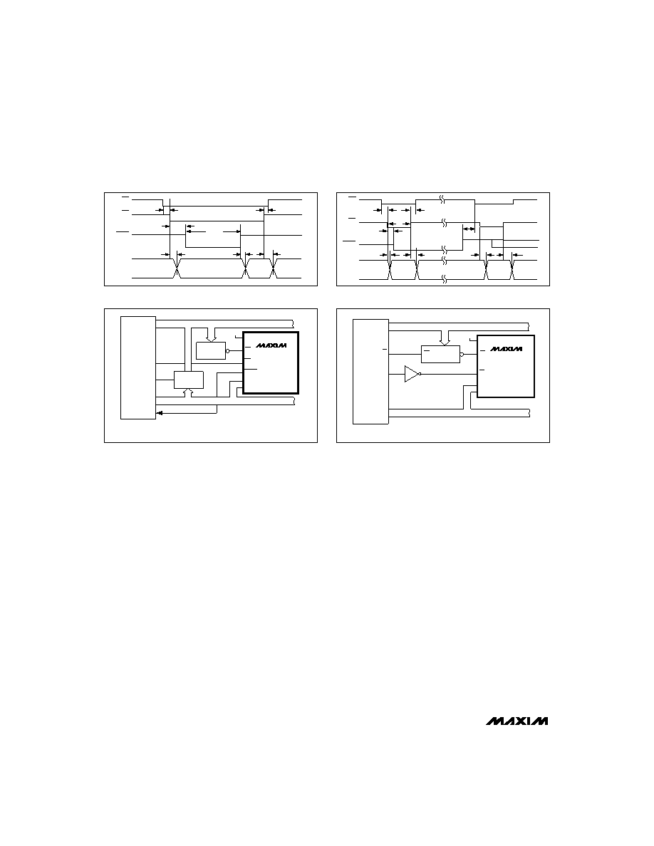
including the 8085A-2, test the status of the READY
input immediately after the start of an instruction cycle.
Therefore, if the MX7575/MX7576 are to be effective in
placing the P in a wait state, their
BUSY output should
go low very early in the cycle. When using the 8085A-2,
the earliest possible indication of an upcoming read
operation is provided by the S0 status signal. Thus, S0,
which is low for a read cycle, should be connected to
the
RD input of the MX7575/MX7576. Figure 4 shows
the connection diagram for the 8085A-2 to the
MX7575/MX7576 in slow-memory interface mode.
ROM Interface Mode
Figure 5 shows the timing diagram for ROM interface
mode. In this mode, the P does not need to be placed
in a wait state. A conversion is started with a read
instruction (
RD and CS go low), and old data is
accessed. The
BUSY signal then goes low to indicate
the start of a conversion. As before, the MX7575
track/hold acquires the signal on the third falling clock
edge after
RD goes low, while the MX7576 samples it
eight times during a conversion. At the end of a conver-
sion (
BUSY going high), another read instruction always
accesses the new data and normally starts a second
conversion. However, if
RD and CS go low within one
external clock period of
BUSY going high, then the sec-
ond conversion is not started. Furthermore, for correct
operation in this mode,
RD and CS should not go low
before
BUSY returns high.
Figures 6 and 7 show the connection diagrams for
interfacing the MX7575/MX7576 in the ROM interface
mode. Figure 6 shows the connection diagram for the
6502/6809 Ps, and Figure 7 shows the connections for
the Z-80.
Due to their fast interface timing, the MX7575/MX7576
will interface to the TMS32010 running at up to 18MHz.
Figure 8 shows the connection diagram for the
TMS32010. In this example, the MX7575/MX7576 are
mapped as a port address. A conversion is initiated by
using an IN A and a PA instruction, and the conversion
result is placed in the TMS32010 accumulator.
Asynchronous Conversion Mode (MX7576)
Tying the MODE pin low places the MX7576 into a con-
tinuous conversion mode. The
RD and CS inputs are
only used for reading data from the converter. Figure 9
shows the timing diagram for this mode of operation,
and Figure 10 shows the connection diagram for the
8085A. In this mode, the MX7576 looks like a ROM to
CMOS, P-Compatible, 5s/10s, 8-Bit ADCs
6
_______________________________________________________________________________________
Figure 3. Slow-Memory Interface Timing Diagram
CS
RD
BUSY
DATA
HIGH-
IMPEDANCE
BUS
HIGH-
IMPEDANCE
BUS
OLD DATA
NEW
DATA
t1
t5
tCONV
t2
t3
t6
t7
Figure 4. MX7575/MX7576 to 8085A-2 Slow-Memory Interface
ADDRESS
DECODE
ADDRESS BUS
+5V
DATA BUS
ADDRESS
LATCH
8085A-2
A8–A15
S0
RD
CS
TP/MODE
BUSY
D0–D7
ALE
AD0–AD7
READY
MX7575*
MX7576
* SOME CIRCUITRY OMITTED FOR CLARITY
S0 IS LOW FOR READ CYCLES
Figure 5. ROM Interface Timing Diagram
CS
RD
BUSY
DATA
HIGH-
IMPEDANCE
BUS
HIGH-
IMPEDANCE
BUS
OLD
DATA
t1
t5
t4
t2
t3
t7
HIGH-IMPEDANCE BUS
NEW
DATA
t8
t3
t7
Figure 6. MX7575/MX7576 to 6502/6809 ROM Interface
ADDRESS
DECODE
ADDRESS BUS
+5V
DATA BUS
6502-6809
A0–A15
R/W
Φ2 OR E
RD
CS
EN
TP/MODE
D0–D7
MX7575*
MX7576
* SOME CIRCUITRY OMITTED FOR CLARITY
相关PDF资料 |
PDF描述 |
|---|---|
| MS27473E10F5PA | CONN PLUG 5POS STRAIGHT W/PINS |
| ICL3232ECV-16Z-T7A | IC TXRX RS232 DUAL ESD 16TSSOP |
| IDT723673L15PF | IC FIFO SYNC 8192X36 128QFP |
| MX7576KP+T | IC ADC 8BIT MPU COMP 20-PLCC |
| IDT72V293L7-5PF8 | IC FIFO 65536X18 7-5NS 80QFP |
相关代理商/技术参数 |
参数描述 |
|---|---|
| MX7575JN | 功能描述:模数转换器 - ADC RoHS:否 制造商:Texas Instruments 通道数量:2 结构:Sigma-Delta 转换速率:125 SPs to 8 KSPs 分辨率:24 bit 输入类型:Differential 信噪比:107 dB 接口类型:SPI 工作电源电压:1.7 V to 3.6 V, 2.7 V to 5.25 V 最大工作温度:+ 85 C 安装风格:SMD/SMT 封装 / 箱体:VQFN-32 |
| MX7575JN+ | 功能描述:模数转换器 - ADC 8-Bit Precision DAC RoHS:否 制造商:Texas Instruments 通道数量:2 结构:Sigma-Delta 转换速率:125 SPs to 8 KSPs 分辨率:24 bit 输入类型:Differential 信噪比:107 dB 接口类型:SPI 工作电源电压:1.7 V to 3.6 V, 2.7 V to 5.25 V 最大工作温度:+ 85 C 安装风格:SMD/SMT 封装 / 箱体:VQFN-32 |
| MX7575JP | 功能描述:模数转换器 - ADC RoHS:否 制造商:Texas Instruments 通道数量:2 结构:Sigma-Delta 转换速率:125 SPs to 8 KSPs 分辨率:24 bit 输入类型:Differential 信噪比:107 dB 接口类型:SPI 工作电源电压:1.7 V to 3.6 V, 2.7 V to 5.25 V 最大工作温度:+ 85 C 安装风格:SMD/SMT 封装 / 箱体:VQFN-32 |
| MX7575JP+ | 功能描述:模数转换器 - ADC 8-Bit Precision DAC RoHS:否 制造商:Texas Instruments 通道数量:2 结构:Sigma-Delta 转换速率:125 SPs to 8 KSPs 分辨率:24 bit 输入类型:Differential 信噪比:107 dB 接口类型:SPI 工作电源电压:1.7 V to 3.6 V, 2.7 V to 5.25 V 最大工作温度:+ 85 C 安装风格:SMD/SMT 封装 / 箱体:VQFN-32 |
| MX7575JP+T | 功能描述:模数转换器 - ADC 8-Bit Precision DAC RoHS:否 制造商:Texas Instruments 通道数量:2 结构:Sigma-Delta 转换速率:125 SPs to 8 KSPs 分辨率:24 bit 输入类型:Differential 信噪比:107 dB 接口类型:SPI 工作电源电压:1.7 V to 3.6 V, 2.7 V to 5.25 V 最大工作温度:+ 85 C 安装风格:SMD/SMT 封装 / 箱体:VQFN-32 |
发布紧急采购,3分钟左右您将得到回复。