- 您现在的位置:买卖IC网 > PDF目录230133 > NAND08GR4B3AN6E (NUMONYX) 512M X 16 FLASH 1.8V PROM, 35 ns, PDSO48 PDF资料下载
参数资料
| 型号: | NAND08GR4B3AN6E |
| 厂商: | NUMONYX |
| 元件分类: | PROM |
| 英文描述: | 512M X 16 FLASH 1.8V PROM, 35 ns, PDSO48 |
| 封装: | 12 X 20 MM, ROHS COMPLIANT, PLASTIC, TSOP-48 |
| 文件页数: | 11/59页 |
| 文件大小: | 998K |
| 代理商: | NAND08GR4B3AN6E |
第1页第2页第3页第4页第5页第6页第7页第8页第9页第10页当前第11页第12页第13页第14页第15页第16页第17页第18页第19页第20页第21页第22页第23页第24页第25页第26页第27页第28页第29页第30页第31页第32页第33页第34页第35页第36页第37页第38页第39页第40页第41页第42页第43页第44页第45页第46页第47页第48页第49页第50页第51页第52页第53页第54页第55页第56页第57页第58页第59页
19/59
NAND512-B, NAND01G-B, NAND02G-B, NAND04G-B, NAND08G-B
DEVICE OPERATIONS
The following section gives the details of the de-
vice operations.
Read Memory Array
At Power-Up the device defaults to Read mode.
To enter Read mode from another mode the Read
command
must
be
issued,
see
10., Commands. Once a Read command is is-
sued, subsequent consecutive Read commands
only require the confirm command code (30h).
Once a Read command is issued two types of op-
erations are available: Random Read and Page
Read.
Random Read. Each time the Read command is
issued the first read is Random Read.
Page Read. After the first Random Read access,
the page data (2112 Bytes or 1056 Words) is
transferred to the Page Buffer in a time of tWHBH
(refer to Table 25. for value). Once the transfer is
complete the Ready/Busy signal goes High. The
data can then be read out sequentially (from se-
lected column address to last column address) by
pulsing the Read Enable signal.
The device can output random data in a page, in-
stead of the consecutive sequential data, by issu-
ing a Random Data Output command.
The Random Data Output command can be used
to skip some data during a sequential data output.
The sequential operation can be resumed by
changing the column address of the next data to
be output, to the address which follows the Ran-
dom Data Output command.
The Random Data Output command can be is-
sued as many times as required within a page.
The Random Data Output command is not accept-
ed during Cache Read operations.
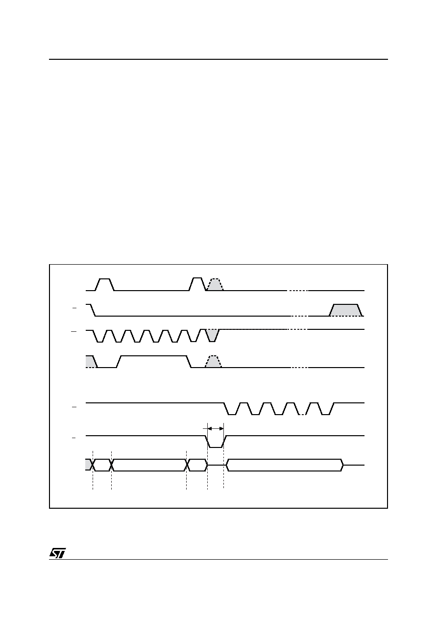
Figure 9. Read Operations
Note: 1. Highest address depends on device density.
CL
E
W
AL
R
I/O
RB
00h
ai08657b
Busy
Command
Code
Data Output (sequentially)
Address Input
tBLBH1
30h
Command
Code
相关PDF资料 |
PDF描述 |
|---|---|
| NAND128W4A2BN1E | 8M X 16 FLASH 3V PROM, 35 ns, PDSO48 |
| NAND256R4A2AN6E | 16M X 16 FLASH 1.8V PROM, 12000 ns, PDSO48 |
| NAND256R4A2CV6F | 16M X 16 FLASH 1.8V PROM, 12000 ns, PDSO48 |
| NAND256W3A0AN6F | 32M X 8 FLASH 3V PROM, 35 ns, PDSO48 |
| NAND512W3A0AN1T | 64M X 8 FLASH 3V PROM, 35 ns, PDSO48 |
相关代理商/技术参数 |
参数描述 |
|---|---|
| NAND08GW3B2AN6E | 功能描述:闪存 4 GBit 2112 Byte 1056 WP 1.8v/3v RoHS:否 制造商:ON Semiconductor 数据总线宽度:1 bit 存储类型:Flash 存储容量:2 MB 结构:256 K x 8 定时类型: 接口类型:SPI 访问时间: 电源电压-最大:3.6 V 电源电压-最小:2.3 V 最大工作电流:15 mA 工作温度:- 40 C to + 85 C 安装风格:SMD/SMT 封装 / 箱体: 封装:Reel |
| NAND08GW3B2AN6F | 功能描述:闪存 4 GB 2112B 1056 Word Pg 1.8V/3V RoHS:否 制造商:ON Semiconductor 数据总线宽度:1 bit 存储类型:Flash 存储容量:2 MB 结构:256 K x 8 定时类型: 接口类型:SPI 访问时间: 电源电压-最大:3.6 V 电源电压-最小:2.3 V 最大工作电流:15 mA 工作温度:- 40 C to + 85 C 安装风格:SMD/SMT 封装 / 箱体: 封装:Reel |
| NAND08GW3B2BN6E | 制造商:Micron Technology Inc 功能描述:NAND & S.MEDIA FLASH - Trays |
| NAND08GW3B2CN6E | 功能描述:闪存 NAND & S.MEDIA FLASH RoHS:否 制造商:ON Semiconductor 数据总线宽度:1 bit 存储类型:Flash 存储容量:2 MB 结构:256 K x 8 定时类型: 接口类型:SPI 访问时间: 电源电压-最大:3.6 V 电源电压-最小:2.3 V 最大工作电流:15 mA 工作温度:- 40 C to + 85 C 安装风格:SMD/SMT 封装 / 箱体: 封装:Reel |
| NAND08GW3B2CN6F | 功能描述:闪存 NAND & S.MEDIA FLASH RoHS:否 制造商:ON Semiconductor 数据总线宽度:1 bit 存储类型:Flash 存储容量:2 MB 结构:256 K x 8 定时类型: 接口类型:SPI 访问时间: 电源电压-最大:3.6 V 电源电压-最小:2.3 V 最大工作电流:15 mA 工作温度:- 40 C to + 85 C 安装风格:SMD/SMT 封装 / 箱体: 封装:Reel |
发布紧急采购,3分钟左右您将得到回复。