- 您现在的位置:买卖IC网 > PDF目录230133 > NAND512W3A2DZA6T (STMICROELECTRONICS) 64M X 8 FLASH 3V PROM, 12000 ns, PBGA63 PDF资料下载
参数资料
| 型号: | NAND512W3A2DZA6T |
| 厂商: | STMICROELECTRONICS |
| 元件分类: | PROM |
| 英文描述: | 64M X 8 FLASH 3V PROM, 12000 ns, PBGA63 |
| 封装: | 8.50 X 15 MM, 1 MM HEIGHT, 0.80 MM PITCH, VFBGA-63 |
| 文件页数: | 2/5页 |
| 文件大小: | 150K |
| 代理商: | NAND512W3A2DZA6T |
2/5
SUMMARY DESCRIPTION
The NAND Flash 528 Byte/ 264 Word Page is a
family of non-volatile Flash memories that uses
NAND cell technology. The devices range from
128Mbits to 1Gbit and operate with either a 1.8V
or 3V voltage supply. The size of a Page is either
528 Bytes (512 + 16 spare) or 264 Words (256 + 8
spare) depending on whether the device has a x8
or x16 bus width.
The address lines are multiplexed with the Data In-
put/Output signals on a multiplexed x8 or x16 In-
put/Output bus. This interface reduces the pin
count and makes it possible to migrate to other
densities without changing the footprint.
Each block can be programmed and erased over
100,000 cycles. To extend the lifetime of NAND
Flash devices it is strongly recommended to imple-
ment an Error Correction Code (ECC). A Write
Protect pin is available to give a hardware protec-
tion against program and erase operations.
The devices feature an open-drain Ready/Busy
output that can be used to identify if the Program/
Erase/Read (P/E/R) Controller is currently active.
The use of an open-drain output allows the Ready/
Busy pins from several memories to be connected
to a single pull-up resistor.
A Copy Back command is available to optimize the
management of defective blocks. When a Page
Program operation fails, the data can be pro-
grammed in another page without having to re-
send the data to be programmed.
Each device has a Cache Program feature which
improves the program throughput for large files. It
loads the data in a Cache Register while the pre-
vious data is transferred to the Page Buffer and
programmed into the memory array.
The devices are available in the following packag-
es:
s
TSOP48 12 x 20mm for all products
s
VFBGA63 (8.5x15x1 mm, 6 x 8 ball array,
0.8mm pitch) for the 512Mb product
s
TFBGA63 (8.5x15x1.2 mm, 6 x 8 ball array,
0.8mm pitch) for the 1Gb product
s
VFBGA63 (9x15x1 mm, 6 x 8 ball array, 0.8mm
pitch) for 128Mb and 256Mb products.
Three options are available for the NAND Flash
family:
s
Automatic Page 0 Read after Power-up, which
allows the microcontroller to directly download
the boot code from page 0.
s
Chip Enable Don’t Care, which allows code to
be directly downloaded by a microcontroller, as
Chip Enable transitions during the latency time
do not stop the read operation.
s
A Serial Number, which allows each device to
be uniquely identified. The Serial Number
options is subject to an NDA (Non Disclosure
Agreement) and so not described in the
datasheet. For more details of this option
contact your nearest ST Sales office.
For information on how to order these options refer
to Table 3, Ordering Information Scheme. Devices
are shipped from the factory with Block 0 always
valid and the memory content bits, in valid blocks,
erased to ’1’.
See Table 1, Product List, for all the devices avail-
able in the family.
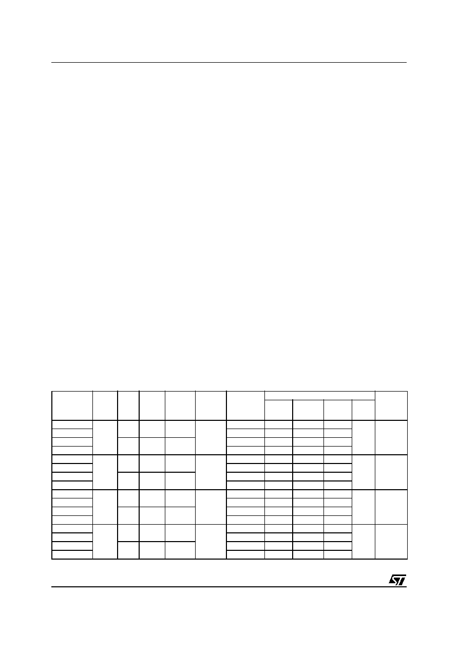
Table 1. Product List
Part Number
Density
Bus
Width
Page Size
Block Size
Memory
Array
Operating
Voltage
Timings
Package
Random
Access
Max
Sequential
Access
Min
Page
Program
Typical
Block
Erase
Typical
NAND128R3A
128Mbit
x8
512+16
Bytes
16K+512
Bytes
32 Pages x
1024 Blocks
1.65 to 1.95V
15s
60ns
300s
2ms
TSOP48
VFBGA63
(9x11x1 mm)
NAND128W3A
2.7 to 3.6V
12s
50ns
200s
NAND128R4A
x16
256+8
Words
8K+256
Words
1.65 to 1.95V
15s
60ns
300s
NAND128W4A
2.7 to 3.6V
12s
50ns
200s
NAND256R3A
256Mbit
x8
512+16
Bytes
16K+512
Bytes
32 Pages x
2048 Blocks
1.65 to 1.95V
15s
60ns
300s
2ms
TSOP48
VFBGA63
(9x11x1 mm)
NAND256W3A
2.7 to 3.6V
12s
50ns
200s
NAND256R4A
x16
256+8
Words
8K+256
Words
1.65 to 1.95V
15s
60ns
300s
NAND256W4A
2.7 to 3.6V
12s
50ns
200s
NAND512R3A
512Mbit
x8
512+16
Bytes
16K+512
Bytes
32 Pages x
4096 Blocks
1.65 to 1.95V
15s
60ns
300s
2ms
TSOP48
VFBGA63
(8.5x15x1
mm)
NAND512W3A
2.7 to 3.6V
12s
50ns
200s
NAND512R4A
x16
256+8
Words
8K+256
Words
1.65 to 1.95V
15s
60ns
300s
NAND512W4A
2.7 to 3.6V
12s
50ns
200s
NAND01GR3A
1Gbit
x8
512+16
Bytes
16K+512
Bytes
32 Pages x
8192 Blocks
1.65 to 1.95V
15s
60ns
300s
2ms
TSOP48
TFBGA63
(8.5x15x1.2
mm)
NAND01GW3A
2.7 to 3.6V
12s
50ns
200s
NAND01GR4A
x16
256+8
Words
8K+256
Words
1.65 to 1.95V
15s
60ns
300s
NAND01GW4A
2.7 to 3.6V
12s
50ns
200s
相关PDF资料 |
PDF描述 |
|---|---|
| NAND512W4A0DN1F | 32M X 16 FLASH 3V PROM, 12000 ns, PDSO48 |
| NAND512W4A2DN6F | 32M X 16 FLASH 3V PROM, 12000 ns, PDSO48 |
| NAND512W4A3CZA1T | 32M X 16 FLASH 3V PROM, 12000 ns, PBGA63 |
| NAND02GW4B3AN6T | 128M X 16 FLASH 3V PROM, 35 ns, PDSO48 |
| NAND02GW4B3BN1 | 128M X 16 FLASH 3V PROM, 35 ns, PDSO48 |
相关代理商/技术参数 |
参数描述 |
|---|---|
| NAND512W3A2SE06 | 制造商:Micron Technology Inc 功能描述:NAND - Gel-pak, waffle pack, wafer, diced wafer on film |
| NAND512W3A2SN6E | 功能描述:IC FLASH 512MBIT 48TSOP RoHS:是 类别:集成电路 (IC) >> 存储器 系列:- 标准包装:1 系列:- 格式 - 存储器:闪存 存储器类型:闪存 - NAND 存储容量:4G(256M x 16) 速度:- 接口:并联 电源电压:2.7 V ~ 3.6 V 工作温度:0°C ~ 70°C 封装/外壳:48-TFSOP(0.724",18.40mm 宽) 供应商设备封装:48-TSOP I 包装:Digi-Reel® 其它名称:557-1461-6 |
| NAND512W3A2SN6F | 制造商:Micron Technology Inc 功能描述:512MB NAND FLASH 制造商:Micron Technology Inc 功能描述:NAND - Tape and Reel |
| NAND512W3A2SZA6E | 制造商:Micron Technology Inc 功能描述:SLC NAND Flash Parallel 3V/3.3V 512Mbit 64M x 8bit 12us 63-Pin VFBGA Tray 制造商:Micron Technology Inc 功能描述:NAND - Trays 制造商:Micron Technology Inc 功能描述:MICNAND512W3A2SZA6E 512MB NAND FLASH 制造商:Micron Technology 功能描述:SLC NAND Flash Parallel 3V/3.3V 512Mbit 64M x 8bit 12us 63-Pin VFBGA Tray |
| NAND512W3A2SZA6F | 制造商:Micron Technology Inc 功能描述:SLC NAND Flash Parallel 3V/3.3V 512Mbit 64M x 8bit 12us 63-Pin VFBGA T/R 制造商:Micron Technology Inc 功能描述:NAND - Tape and Reel 制造商:Micron Technology 功能描述:SLC NAND Flash Parallel 3V/3.3V 512Mbit 64M x 8bit 12us 63-Pin VFBGA T/R |
发布紧急采购,3分钟左右您将得到回复。