参数资料
| 型号: | NB4N11MDTEVB |
| 厂商: | ON Semiconductor |
| 文件页数: | 3/6页 |
| 文件大小: | 0K |
| 描述: | BOARD EVAL FOR NB4N11MD |
| 设计资源: | NB4N11MDTEVB Gerber Files |
| 标准包装: | 1 |
| 系列: | * |
�� �
�
�NB4N11MDTEVB�
�NC�
�SMA_GND�
�NC�
�SMA_GND�
�V� CC�
�V� CC�
�V� EE�
�V� EE�
�V� EE�
�V� CC�
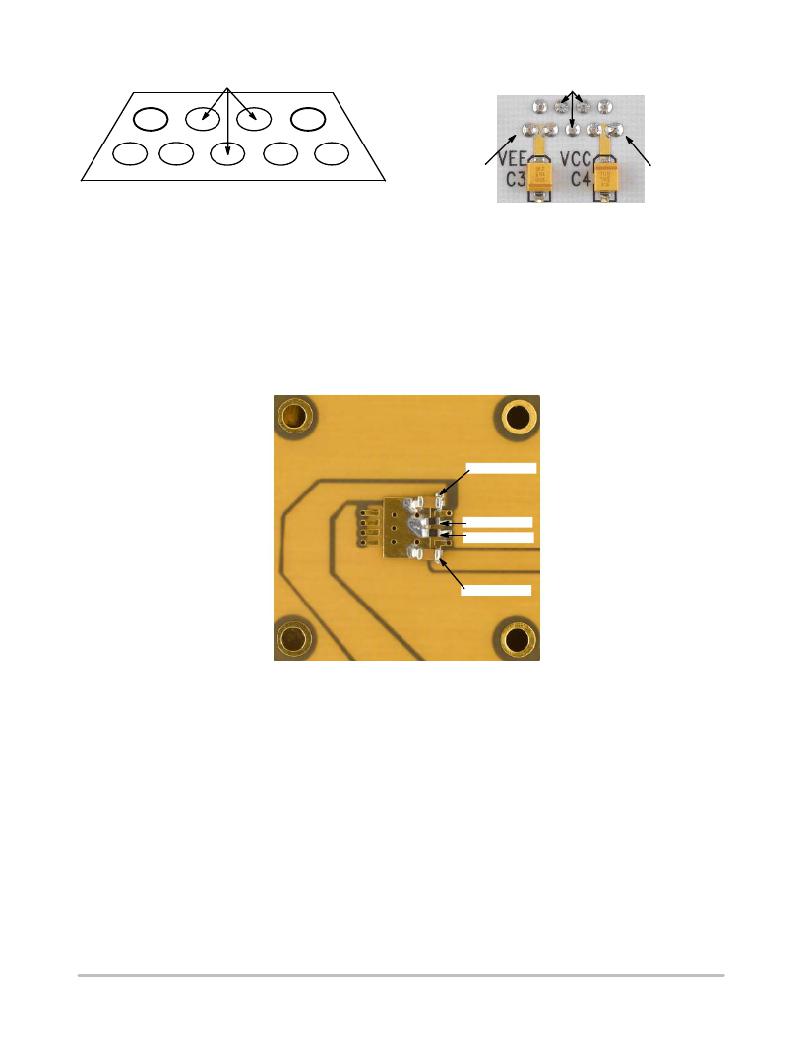
�C3� =� 10� m� F;� C4� =� 10� m� F�
�Figure� 4.� Power� Supply� Connector� ?� 9� Pin� Side�
�View� (Left)� and� PCB� Top� View� (Right)�
�Stimulus� (Generator)� Termination�
�All� ECL� outputs� need� to� be� terminated� to� V� TT� (V� TT� =�
�V� CC� –� 2.0� V� =� GND)� via� a� 50� W� resistor.� The� current� board�
�design� utilizes� the� space� for� placement� of� the� external�
�termination� resistors.� (More� information� on� termination� is�
�provided� in� AN8020).� The� 0402� chip� resistor� pads� are�
�provided� on� the� bottom� side� of� the� evaluation� board.� Solder�
�the� chip� resistors� to� the� bottom� side� of� the� board� between� the�
�appropriate� input� of� the� device� pin� pads� and� the� ground� pads�
�as� shown� in� Figure� 5� (for� split� power� supply� setup,� PCB� is�
�assembled� in� this� configuration).�
�C1� =� 0.01� m� F�
�R2� =� 50� W�
�R1� =� 50� W�
�C2� =� 0.01� m� F�
�Figure� 5.� Expanded� Bottom� View�
�Likewise� for� CML� outputs,� CML� stimulus� signal� need� to�
�be� terminated� to� V� CC� via� a� 50� W� resistor.� To� accomplish� this�
�configuration� the� external� termination� resistor� has� to� be�
�moved� from� SMA_GND� ring� to� V� CC� ring� on� the� bottom� of�
�the� board.�
�For� the� LVDS� configuration� Input� pin� pads� of� the� D0� or�
�D1� input� has� to� be� shorted� using� 100� W� resistor� across�
�differential� lines.�
�oscilloscope� to� be� used� as� a� termination� of� the� signals� (in�
�split� power� supply� setup� SMA_GND� as� a� system� ground,�
�V� CC� ,� and� V� EE� are� varied;� see� Table� 1,� Power� Supply� Levels).�
�Board� Components� Configuration�
�The� NB4N11MDTEVB� evaluation� board� requires� six�
�side� SMA� connectors.� Placement� locations� are� described� in�
�the� Table� 2� below.�
�DUT� Termination�
�For� standard� lab� setup� and� test,� a� split� (dual)� power� supply�
�is� required� enabling� the� 50� W� internal� impedance� in� the�
�http://onsemi.com�
�3�
�相关PDF资料 |
PDF描述 |
|---|---|
| NB4N441MNGEVB | BOARD EVAL NB4N441MNG |
| NB4N507ADEVB | BOARD EVAL FOR BBG NB4N507AD |
| NB4N855SMEVB | CUSTOMER EVALUATION BRD |
| NB6L11MMNGEVB | BOARD EVAL NB6L11MMN CLK BUFFER |
| NB6L239MNEVB | BOARD EVAL BBG NB6L239MND |
相关代理商/技术参数 |
参数描述 |
|---|---|
| NB4N11MDTG | 功能描述:时钟缓冲器 MLTLVL IN-CML RECBUF RoHS:否 制造商:Texas Instruments 输出端数量:5 最大输入频率:40 MHz 传播延迟(最大值): 电源电压-最大:3.45 V 电源电压-最小:2.375 V 最大功率耗散: 最大工作温度:+ 85 C 最小工作温度:- 40 C 封装 / 箱体:LLP-24 封装:Reel |
| NB4N11MDTR2G | 功能描述:时钟缓冲器 MLTLVL IN-CML RECBUF RoHS:否 制造商:Texas Instruments 输出端数量:5 最大输入频率:40 MHz 传播延迟(最大值): 电源电压-最大:3.45 V 电源电压-最小:2.375 V 最大功率耗散: 最大工作温度:+ 85 C 最小工作温度:- 40 C 封装 / 箱体:LLP-24 封装:Reel |
| NB4N11SMNG | 功能描述:时钟缓冲器 LVDS FANOUT BUFF/ TRANS RoHS:否 制造商:Texas Instruments 输出端数量:5 最大输入频率:40 MHz 传播延迟(最大值): 电源电压-最大:3.45 V 电源电压-最小:2.375 V 最大功率耗散: 最大工作温度:+ 85 C 最小工作温度:- 40 C 封装 / 箱体:LLP-24 封装:Reel |
| NB4N11SMNR2G | 功能描述:时钟缓冲器 LVDS FANOUT BUFF/ TRANS RoHS:否 制造商:Texas Instruments 输出端数量:5 最大输入频率:40 MHz 传播延迟(最大值): 电源电压-最大:3.45 V 电源电压-最小:2.375 V 最大功率耗散: 最大工作温度:+ 85 C 最小工作温度:- 40 C 封装 / 箱体:LLP-24 封装:Reel |
| NB4N121K | 制造商:ONSEMI 制造商全称:ON Semiconductor 功能描述:3.3V Differential In 1:21 Differential Fanout Clock Driver with HCSL level Output |
发布紧急采购,3分钟左右您将得到回复。