- 您现在的位置:买卖IC网 > PDF目录11784 > NCN8024DWR2G (ON Semiconductor)IC SMART CARD IC2 28SOIC PDF资料下载
参数资料
| 型号: | NCN8024DWR2G |
| 厂商: | ON Semiconductor |
| 文件页数: | 2/16页 |
| 文件大小: | 0K |
| 描述: | IC SMART CARD IC2 28SOIC |
| 标准包装: | 1,000 |
| 应用: | 智能卡读取器,写入器 |
| 电源电压: | 5V |
| 封装/外壳: | 28-SOIC(0.295",7.50mm 宽) |
| 供应商设备封装: | 28-SOIC W |
| 包装: | 带卷 (TR) |
| 安装类型: | 表面贴装 |
| 其它名称: | NCN8024DWR2G-ND NCN8024DWR2GOSTR |
NCN8024
http://onsemi.com
10
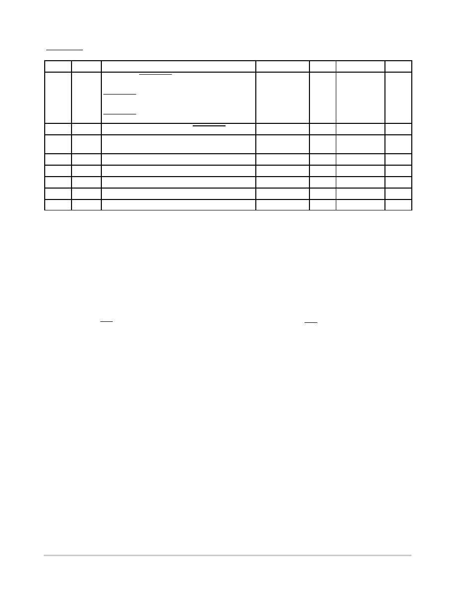
SMART CARD INTERFACE SECTION, CRD_IO, CRD_AUX1, CRD_AUX2, CRD_CLK, CRD_RST, CRD_PRES,
CRD_PRES (VDD = 3.3 V; VDDP = 5 V; Tamb = 25°C; FCLKIN = 10 MHz)
Pin
Unit
Max
Typ
Min
Rating
Symbol
9, 10
|IIH|
|IIL|
CRD_PRES, CRD_PRES
High level input leakage current, VIH = VDD
CRD_PRES
Low level input leakage current, VIL = 0 V
CRD_PRES
5
10
1
10
mA
9, 10
5
8
11
ms
11, 12,
13, 16
ICRD_IO CRD_IO, CRD_AUX1, CRD_AUX2 Current Limitation
15
mA
15
ICRD_CLK CRD_CLK Current Limitation
70
mA
16
ICRD_RST CRD_RST Current Limitation
20
mA
tact
Activation Time (Note 7)
30
100
ms
tdeact
Deactivation Time (Note 7)
30
250
ms
Temp SD Shutdown Temperature
160
°C
NOTE: Device will meet the specifications after thermal equilibrium has been established when mounted in a test socket or printed
circuit board with maintained transverse airflow greater than 500 lfpm. Electrical parameters are guaranteed only over the
declared operating temperature range. Functional operation of the device exceeding these conditions is not implied. Device
specification limit values are applied individually under normal operating conditions and not valid simultaneously.
7. Guaranteed by design and characterization
POWER SUPPLY
The NCN8024 smart card interface has two power
supplies: VDD and VDDP.
VDD is usually common to the system controller and the
interface. The applied VDD ranges from 2.7 V up to 5.5 V.
If VDD goes below 2.35 V typical (UVLOVDD) a
powerdown sequence is automatically performed. In that
case the interrupt (INT) pin is set Low.
A builtin chargepumpbased DC/DC converter
followed by a Low DropOut (LDO) regulator is used to
provide the 3 V or 5 V power supply voltage (CRD_VCC) to
the card. VDDP is the converter’s input voltage. VUP is the
chargepump converter’s output. It is connected to the LDO
input. A reservoir capacitor of 100 nF is connected to VUP.
CRD_VCC is the LDO output. Even if the converter can
operate with a single output reservoir capacitor as low as
100 nF at CRD_VCC, it is recommended to use a capacitor
of at least 320 nF in order to satisfy the datasheet
specifications. The best recommended combination
guaranteeing optimal performances consists in a distributed
set of capacitors 220 nF + 330 nF (in particular
recommended for optimally satisfying the NDS standard).
To minimize dI/dt effects, the fly capacitor (100 nF) and the
reservoir capacitors VUP and CRD_VCC have to be
connected as close as possible to the corresponding device’s
pin and feature very low ESR values (lower than 50 m
W).
The fly capacitor is connected between C1 and C2. The
decoupling capacitors on VDD and VDDP respectively
100 nF and 10
mF have also to be connected close to the
respective IC pins.
The CRD_VCC pin can source up to 75 mA continuously
over the VDDP range (from 3.3 V to 5.5 V), the absolute
maximum current being internally limited below 150 mA
(Typical at 110 mA). CRD_VCC can stay in the range 4.6 V
– 5.30 V during current transient up to 200 mA (peak
current) over less than 400 ns of current pulse duration such
as the charge transient is lower than 40 nAs.
There’s no specific sequence for applying VDD or VDDP.
They can be applied to the interface in any sequence. After
powering the device INT remains Low until a card is
inserted.
SUPPLY VOLTAGE MONITORING
The supply voltage monitoring block includes the Power
On Reset (POR) circuitry and the under voltage lockout
(UVLO) detection (VDD voltage dropout detection).
PORADJ pin allows the user, according to the considered
application, to adjust the VDD UVLO threshold. If not used
PORADJ pin is connected to Ground.
The input supply voltage is continuously monitored to
prevent under voltage operation. At power up, the system
initializes the internal logic during POR timing and no
further signal can be provided or supported during this
period. Such initialization takes place when the input
voltage rises between 2 V to 2.6 V about typical.
The system is ready to operate when the input voltage has
reached the minimum 2.7 V. Considering this, the NCN8024
will detect an UnderVoltage situation when the input
supply voltage will drop below 2.35 V typical. When VDD
goes down below the UVLO falling threshold a deactivation
sequence is performed.
The device is inactive during poweron and poweroff of
the VDD supply (8 ms reset pulse).
相关PDF资料 |
PDF描述 |
|---|---|
| TSI148-133IL | IC PCI-VME BRIDGE 456PBGA |
| IDTTSI148-133ILY | IC PCI/X TO VMEBUS BRIDGE |
| 1604050-5 | 350A HOUSING SUB-ASSY,BLUE |
| 1604037-1 | CONN HOUSING 2-POLE 175AMP YEL |
| 1986000-2 | CONN HOUSING ASSY SERIES 75 RED |
相关代理商/技术参数 |
参数描述 |
|---|---|
| NCN8024RDWR2G | 功能描述:接口 - 专用 SMART CARD IC RoHS:否 制造商:Texas Instruments 产品类型:1080p60 Image Sensor Receiver 工作电源电压:1.8 V 电源电流:89 mA 最大功率耗散: 最大工作温度:+ 85 C 安装风格:SMD/SMT 封装 / 箱体:BGA-59 |
| NCN8025 | 制造商:ONSEMI 制造商全称:ON Semiconductor 功能描述:Compact SMART CARD Interface IC |
| NCN8025A-EVB | 制造商:ON Semiconductor 功能描述:Evaluation board for 1.8V/3V/5V Smart Card Interface 制造商:P&S 功能描述:Evaluation board for 1.8V/3V/5V Smart Card Interface |
| NCN8025AMNGEVB | 功能描述:电源管理IC开发工具 NCN8025AMNTXG RoHS:否 制造商:Maxim Integrated 产品:Evaluation Kits 类型:Battery Management 工具用于评估:MAX17710GB 输入电压: 输出电压:1.8 V |
| NCN8025AMNTXG | 功能描述:接口 - 专用 SMART CARD IC RoHS:否 制造商:Texas Instruments 产品类型:1080p60 Image Sensor Receiver 工作电源电压:1.8 V 电源电流:89 mA 最大功率耗散: 最大工作温度:+ 85 C 安装风格:SMD/SMT 封装 / 箱体:BGA-59 |
发布紧急采购,3分钟左右您将得到回复。