- 您现在的位置:买卖IC网 > PDF目录11784 > NCN8024DWR2G (ON Semiconductor)IC SMART CARD IC2 28SOIC PDF资料下载
参数资料
| 型号: | NCN8024DWR2G |
| 厂商: | ON Semiconductor |
| 文件页数: | 3/16页 |
| 文件大小: | 0K |
| 描述: | IC SMART CARD IC2 28SOIC |
| 标准包装: | 1,000 |
| 应用: | 智能卡读取器,写入器 |
| 电源电压: | 5V |
| 封装/外壳: | 28-SOIC(0.295",7.50mm 宽) |
| 供应商设备封装: | 28-SOIC W |
| 包装: | 带卷 (TR) |
| 安装类型: | 表面贴装 |
| 其它名称: | NCN8024DWR2G-ND NCN8024DWR2GOSTR |
NCN8024
http://onsemi.com
11
PORADJ pin is used to modify the UVLO threshold
according to the below relationship considering an external
resistor divider R1 / R2 (see block diagram Figure 1):
UVLO + R1 ) R2
R2
VPOR
If PORADJ is connected to Ground the VDD UVLO
threshold (VDD falling) is typically 2.35 V. In some cases it
can be interesting to adjust this threshold at a higher value
and by the way increase the VDD supply dropout detection
level which enables a deactivation sequence if the VDD
voltage is too low.
For example, there are microcontrollers for which the
minimum supply voltage insuring a correct operating is
higher than 2.55 V, increasing UVLOVDD (VDD falling) is
consequently necessary. Considering for instance a resistor
bridge with R1 = 56 k
W, R2 = 42 kW and VPOR = 1.18 V
typical the VDD dropout detection level can be increased up to:
UVLO + 59k ) 42k
42k
VPOR + 2.75 V
The minimum dropout detection voltage should be higher
than 2 V.
The maximum detection level may be up to VDD.
CLOCK DIVIDER:
The input clock can be divided by 1/1, 1/2, 1/4, or 1/8,
depending upon the specific application, prior to be applied
to the smart card driver. These division ratios are
programmed using pins CLKDIV1 and CLKDIV2 (see
Table 1). The input clock is provided externally to pin
CLKIN.
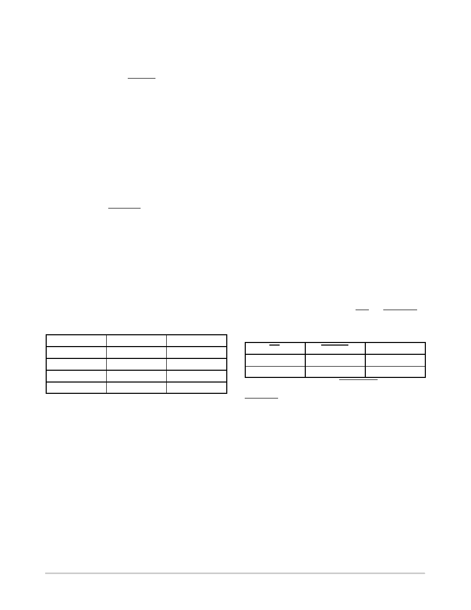
Table 1. Clock Frequency Programming
CLKDIV1
CLKDIV2
FCRD_CLK
0
CLKIN/8
0
1
CKLKIN / 4
1
0
CLKIN
1
CLKIN / 2
The clock input stage (CLKIN) can handle a 27 MHz
maximum frequency signal (considering a division ratio
w
2). Of course, the ratio must be defined by the user to cope
with Smart Card considered in a given application
In order to avoid any duty cycle out of the 45% / 55%
range specification, the divider is synchronized by the last
flip flop, thus yielding a constant 50% duty cycle, whatever
be the divider ratio 1/2, 1/4 or 1/8. On the other hand, the
output signal Duty Cycle cannot be guaranteed 50% if the
division ratio is 1 and if the input Duty Cycle signal is not
within the 46 56% range at the CLKIN input.
When the signal applied to CLKIN is coming from the
external controller, the clock will be applied to the card
under the control of the microcontroller or similar device
after the activation sequence has been completed.
DATA I/O, AUX1 and AUX2 LEVEL SHIFTERS
The three bidirectional level shifters I/O, AUX1 and
AUX2 adapt the voltage difference that might exist between
the microcontroller and the smart card. These three
channels are identical. The first side of the bidirectional
level shifter dropping Low (falling edge) becomes the driver
side until the level shifter enters again in the idle state pulling
High CRD_IO and I/Ouc.
Passive 11 k
W pullup resistors have been internally
integrated on each terminal of the bidirectional channel. In
addition with these pullup resistors, an active pullup
circuit provides a fast charge of the stray capacitance.
The current to and from the card I/O lines is limited
internally to 15 mA and the maximum frequency on these
lines is 1 MHz.
STANDBY MODE
After a Poweron reset, the circuit enters the standby
mode. A minimum number of circuits are active while
waiting for the microcontroller to start a session:
All card contacts are inactive
Pins I/Ouc, AUX1uc and AUX2uc are in the
highimpedance state (11 k
W pullup resistor to VDD)
Card pins are inactive and pulled Low
Supply Voltage monitoring is active
The internal DC/DC converter oscillator is running.
POWERUP
In the standby mode the microcontroller can check the
presence of a card using the signals INT and CMDVCC as
shown in Table 2:
Table 2. Card Presence State
INT
CMDVCC
State
HIGH
Card present
LOW
HIGH
Card not present
If a card is detected present (CRD_PRES or CRD_PRES
active) the controller can start a card session by pulling
CMDVCC Low. Card activation is run (t0, Figure 5). This
PowerUp Sequence makes sure all the card related signals
are LOW during the CRD_VCC positive going slope. These
lines are validated when CRD_VCC is stable and above the
minimum voltage specified. When the CRD_VCC voltage
reaches the programmed value (3.0 V or 5.0 V), the circuit
activates the card signals according to the following
sequence (Figure 5):
CRD_VCC is poweredup at its nominal value (t1)
I/O, AUX1 and AUX2 lines are activated (t2)
Then Clock channel is activated and the clock signal is
applied to the card (t3)
Finally the Reset level shifter is enabled (t4)
相关PDF资料 |
PDF描述 |
|---|---|
| TSI148-133IL | IC PCI-VME BRIDGE 456PBGA |
| IDTTSI148-133ILY | IC PCI/X TO VMEBUS BRIDGE |
| 1604050-5 | 350A HOUSING SUB-ASSY,BLUE |
| 1604037-1 | CONN HOUSING 2-POLE 175AMP YEL |
| 1986000-2 | CONN HOUSING ASSY SERIES 75 RED |
相关代理商/技术参数 |
参数描述 |
|---|---|
| NCN8024RDWR2G | 功能描述:接口 - 专用 SMART CARD IC RoHS:否 制造商:Texas Instruments 产品类型:1080p60 Image Sensor Receiver 工作电源电压:1.8 V 电源电流:89 mA 最大功率耗散: 最大工作温度:+ 85 C 安装风格:SMD/SMT 封装 / 箱体:BGA-59 |
| NCN8025 | 制造商:ONSEMI 制造商全称:ON Semiconductor 功能描述:Compact SMART CARD Interface IC |
| NCN8025A-EVB | 制造商:ON Semiconductor 功能描述:Evaluation board for 1.8V/3V/5V Smart Card Interface 制造商:P&S 功能描述:Evaluation board for 1.8V/3V/5V Smart Card Interface |
| NCN8025AMNGEVB | 功能描述:电源管理IC开发工具 NCN8025AMNTXG RoHS:否 制造商:Maxim Integrated 产品:Evaluation Kits 类型:Battery Management 工具用于评估:MAX17710GB 输入电压: 输出电压:1.8 V |
| NCN8025AMNTXG | 功能描述:接口 - 专用 SMART CARD IC RoHS:否 制造商:Texas Instruments 产品类型:1080p60 Image Sensor Receiver 工作电源电压:1.8 V 电源电流:89 mA 最大功率耗散: 最大工作温度:+ 85 C 安装风格:SMD/SMT 封装 / 箱体:BGA-59 |
发布紧急采购,3分钟左右您将得到回复。