参数资料
| 型号: | NCP1031POEEVB |
| 厂商: | ON Semiconductor |
| 文件页数: | 14/19页 |
| 文件大小: | 0K |
| 描述: | BOARD EVAL NCP1031 POE DC CONV |
| 设计资源: | NCP1031POEEVB Schematic NCP1031POEEVB Gerber Files NCP1031POEEVB Bill of Materials |
| 标准包装: | 1 |
| 主要目的: | 电源管理,以太网供电(POE) |
| 嵌入式: | 否 |
| 已用 IC / 零件: | NCP1031 |
| 已供物品: | 板 |
| 其它名称: | NCP1031POEEVB-ND NCP1031POEEVBOS |
�� �
�
�NCP1030,� NCP1031�
�be� limited� by� the� EA� sink� current,� typically� 110� m� A.�
�Optimum� transient� response� is� obtained� if� the� compensation�
�is� discharging,� guaranteeing� a� maximum� duty� cycle� of� 75� %�
�as� shown� in� Figure� 35.�
�components� allow� COMP� to� swing� across� its� operating�
�range� in� 1� cycle.�
�Line� Under� and� Overvoltage� Detector�
�C� T� Ramp�
�COMP�
�Enabled�
�C� T� Charge�
�Signal�
�The� NCP103x� incorporates� individual� line� undervoltage�
�(UV)� and� overvoltage� (OV)� shutdown� circuits.� The� UV� and�
�OV� thresholds� are� 2.5� V.� A� fault� is� present� if� the� UV� is� below�
�2.5� V� or� if� the� OV� voltage� is� above� 2.5� V.� The� UV/OV�
�detectors� incorporate� 175� mV� hysteresis� to� prevent� noise�
�from� triggering� the� shutdown� circuits.�
�The� UV/OV� circuits� can� be� biased� using� an� external�
�resistor� divider� from� the� input� line� as� shown� in� Figure� 34.�
�The� UV/OV� pins� should� be� bypassed� using� a� capacitor� to�
�prevent� triggering� the� UV� or� OV� circuits� during� normal�
�switching� operation.�
�V� in�
�R� 1�
�+�
�R� 2�
�+� V� UV�
�V� OV� R� 3�
�--� --�
�Figure� 34.� UV/OV� Resistor� Divider�
�from� the� Input� Line�
�The� resistor� divider� must� be� sized� to� enable� the� controller�
�Power� Switch� Max�
�Duty� Cycle�
�75%�
�25� %�
�Figure� 35.� Maximum� Duty� Cycle� vs� COMP�
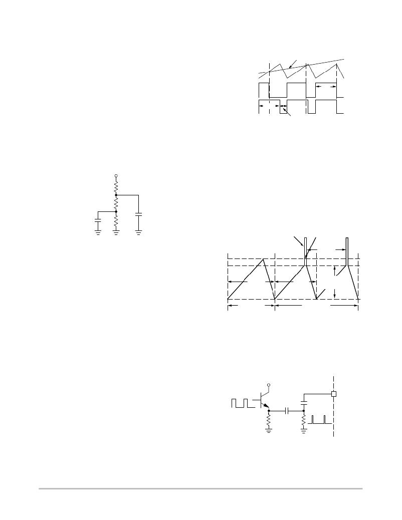
�Figure� 18� shows� the� relationship� between� the� operating�
�frequency� and� C� T� .� If� an� UV� fault� is� present,� both� I� CT(C)� and�
�I� CT(D)� are� reduced� by� a� factor� of� 7,� thus� reducing� the�
�operating� frequency� by� the� same� factor.�
�The� oscillator� can� be� synchronized� to� a� higher� frequency�
�by� capacitively� coupling� a� synchronization� pulse� into� the� C� T�
�pin.� In� sync� mode,� the� voltage� on� the� C� T� pin� needs� to� be�
�driven� above� 3.5� V� to� trigger� the� internal� comparator� and�
�complete� the� C� T� charging� period.� However,� pulsing� the� C� T�
�pin� before� it� reaches� 3.5� V� will� reduce� the� p--p� amplitude� of�
�the� C� T� Ramp� as� shown� in� Figure� 36.�
�3.0� V/3.5� V�
�Sync� Pulse� Comparator�
�Reset�
�T2� (f2)�
�3.5� V�
�once� V� in� is� within� the� required� operating� range.� While� a� UV�
�or� OV� fault� is� present,� switching� is� not� allowed� and� the�
�COMP� pin� is� effectively� grounded.�
�C� T�
�Ramp�
�T1� (f1)�
�T2� (f2)�
�C� T� Voltage�
�Range� in� Sync�
�Either� of� these� comparators� can� be� used� for� a� different�
�function� if� UV� or� OV� functions� are� not� needed.� For� example,�
�the� UV/OV� detectors� can� be� used� to� implement� an� enable� or�
�3.0� V�
�Free� Running�
�Mode�
�Sync� Mode�
�disable� function.� If� positive� logic� is� used,� the� enable� signal�
�is� applied� to� the� UV� pin� while� the� OV� pin� is� grounded.� If�
�negative� logic� is� used,� the� disable� signal� is� applied� to� the� OV�
�pin� while� biasing� the� UV� pin� from� V� CC� using� a� resistor�
�divider.�
�Oscillator�
�Figure� 36.� External� Frequency� Synchronization�
�Waveforms�
�The� oscillator� frequency� should� be� set� no� more� that� 25%�
�below� the� target� sync� frequency� to� maintain� an� adequate�
�voltage� range� and� provide� good� noise� immunity.� A� possible�
�circuit� to� synchronize� the� oscillator� is� shown� in� Figure� 37.�
�The� oscillator� is� optimized� for� operation� up� to� 1� MHz� and�
�its� frequency� is� set� by� the� external� timing� capacitor� (C� T� )�
�connected� to� the� C� T� pin.� The� oscillator� has� two� modes� of�
�operation,� free� running� and� synchronized� (sync).� While� in�
�free� running� mode,� an� internal� current� source� sequentially�
�charges� and� discharges� C� T� generating� a� voltage� ramp�
�between� 3.0� V� and� 3.5� V.� Under� normal� operating�
�conditions,� the� charge� (I� CT(C)� )� and� discharge� (I� CT(D)� )�
�currents� are� typically� 215� m� A� and� 645� m� A,� respectively.� The�
�5V�
�R1�
�C1�
�C� T�
�R2�
�C� T�
�2�
�charge:discharge� current� ratio� of� 1:3� discharges� C� T� in� 25� %�
�of� the� total� period.� The� Power� Switch� is� disabled� while� C� T�
�Figure� 37.� External� Frequency� Synchronization�
�Circuit.�
�http://onsemi.com�
�14�
�相关PDF资料 |
PDF描述 |
|---|---|
| NCP1605LCDTVGEVB | BOARD EVAL NCP1605/1396 |
| NCP1608BOOSTGEVB | BOARD EVAL NCP1608 100W BOOST |
| NCP1631PFCGEVB | BOARD DEMO NCP1631 INTERLEAV PFC |
| NCP1650EVB | BOARD EVAL NCP1650 PFC CTLR |
| NCP1652L48VGEVB | BOARD EVAL 100W 48V NCP1652 PFC |
相关代理商/技术参数 |
参数描述 |
|---|---|
| NCP1034 | 制造商:ONSEMI 制造商全称:ON Semiconductor 功能描述:100V Synchronous PWM Buck Controller |
| NCP1034BCK5VGEVB | 功能描述:电源管理IC开发工具 48/5V 5A SYNC BCK RoHS:否 制造商:Maxim Integrated 产品:Evaluation Kits 类型:Battery Management 工具用于评估:MAX17710GB 输入电压: 输出电压:1.8 V |
| NCP1034DR2G | 功能描述:DC/DC 开关控制器 HV PWM BUCK CONTROLR RoHS:否 制造商:Texas Instruments 输入电压:6 V to 100 V 开关频率: 输出电压:1.215 V to 80 V 输出电流:3.5 A 输出端数量:1 最大工作温度:+ 125 C 安装风格: 封装 / 箱体:CPAK |
| NCP1050 | 制造商:ONSEMI 制造商全称:ON Semiconductor 功能描述:Monolithic High Voltage Gated Oscillator Power Switching Regulator |
| NCP1050/D | 制造商:ONSEMI 制造商全称:ON Semiconductor 功能描述:Monolithic High Voltage Gated Oscillator Power Switching Regulator |
发布紧急采购,3分钟左右您将得到回复。