- 您现在的位置:买卖IC网 > Datasheet目录45 > NCP1083DEG (ON Semiconductor)IC CONV CTLR POE-PD 40W 20-TSSOP Datasheet资料下载
参数资料
| 型号: | NCP1083DEG |
| 厂商: | ON Semiconductor |
| 文件页数: | 6/18页 |
| 文件大小: | 257K |
| 描述: | IC CONV CTLR POE-PD 40W 20-TSSOP |
| 标准包装: | 74 |
| 类型: | 以太网供电开关(PoE) |
| 应用: | 远程外设(工业控制,相机,数据访问) |
| 内部开关: | 是 |
| 电流限制: | 1.1A |
| 电源电压: | 0 V ~ 57 V |
| 工作温度: | -40°C ~ 85°C |
| 安装类型: | 表面贴装 |
| 封装/外壳: | 20-TSSOP(0.173",4.40mm 宽)裸露焊盘 |
| 供应商设备封装: | 20-TSSOP-EP |
| 包装: | 管件 |
NCP1083
http://onsemi.com
6
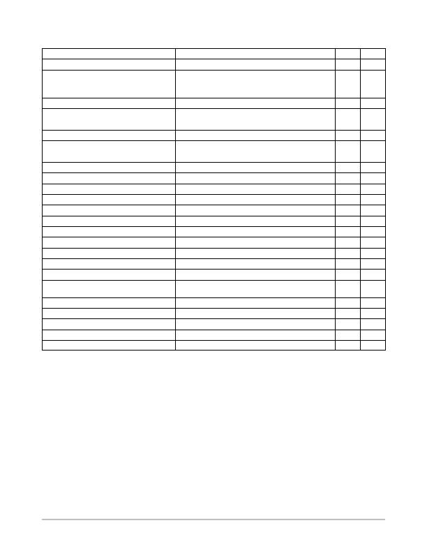
Table 2. ABSOLUTE MAXIMUM RATINGS
Symbol
Parameter
Conditions
Min
Max
Unit
VPORTP
Input power supply
Voltage with respect to VPORTN
1,2
0.3
72
V
RTN
ARTN
Analog ground supply 2
Passswitch in offstate
(Voltage with respect to VPORTN
1,2
)
0.3
72
V
VDDH
Internal regulator output
Voltage with respect to ARTN
0.3
17
V
VDDL
Internal regulator output
Voltage with respect to ARTN
0.3
3.6
V
CLASS
Analog output
Voltage with respect to VPORTN
1,2
0.3
3.6
V
INRUSH
Analog output
Voltage with respect to VPORTN
1,2
0.3
3.6
V
ILIM1
Analog output
Voltage with respect to VPORTN
1,2
0.3
3.6
V
UVLO
Analog input
Voltage with respect to VPORTN
1,2
0.3
3.6
V
OSC
Analog output
Voltage with respect to ARTN
0.3
3.6
V
COMP
Analog input / output
Voltage with respect to ARTN
0.3
3.6
V
FB
Analog input
Voltage with respect to ARTN
0.3
3.6
V
CS
Analog input
Voltage with respect to ARTN
0.3
3.6
V
SS
Analog input
Voltage with respect to ARTN
0.3
3.6
V
nCLASS_AT
Analog output
Voltage with respect to ARTN
0.3
3.6
AUX
Analog input
Voltage with respect to VPORTN
1,2
0.3
3.6
V
TEST
Digital input
Voltage with respect to VPORTN
1,2
0.3
3.6
V
Ta
Ambient temperature
40
85
癈
Tj
Junction temperature
150
癈
TjTSD
Junction temperature (Note 1)
Thermal shutdown condition
175
癈
T
stg
Storage Temperature
55
150
癈
T
窲A
Thermal Resistance,
Junction to Air (Note 2)
Exposed pad connected to VPORTN
1,2
ground
37.6
癈/W
ESDHBM
Human Body Model
per JEDEC Standard JESD22
4
kV
ESDCDM
Charged Device Model
750
V
ESDMM
Machine Model
300
V
LU
Latchup
per JEDEC Standard JESD78
?00
mA
ESDSYS
System ESD (contact/air) (Note 3)
8/15
kV
Stresses exceeding Maximum Ratings may damage the device. Maximum Ratings are stress ratings only. Functional operation above the
Recommended Operating Conditions is not implied. Extended exposure to stresses above the Recommended Operating Conditions may affect
device reliability.
1. TjTSD allowed during error conditions only. It is assumed that this maximum temperature condition does not occur more than 1 hour
cumulative during the useful life for reliability reasons.
2. Mounted on a 1S2P (3 layer) test board with copper coverage of 25 percent for the signal layers and 90 percent copper coverage for the
inner planes at an ambient temperature of 85癈 in still air. Refer to JEDEC JESD517 for details.
3. Surges per EN6100042, 1999 applied between RJ45 and output ground and between adapter input and output ground of the evaluation
board. The specified values are the test levels and not the failure levels.
相关PDF资料 |
PDF描述 |
|---|---|
| NCP1501DMR2G | IC REG SGL BUCK/LINEAR 8MICRO |
| NCP1578MNR2G | IC REG DL BCK/LINEAR SYNC 20-QFN |
| NCP1601BDR2G | IC PFC CTRL CRM/TRANSITION 8SOIC |
| NCP1603D100R2G | IC CTLR PFC/PWM COMBO 16-SOIC |
| NCP1605DR2G | IC PFC CONTROLLER CCM/DCM 16SOIC |
相关代理商/技术参数 |
参数描述 |
|---|---|
| NCP1083DER2G | 功能描述:DC/DC 开关控制器 POE-PD 40W DC-DC AUX SUPP RoHS:否 制造商:Texas Instruments 输入电压:6 V to 100 V 开关频率: 输出电压:1.215 V to 80 V 输出电流:3.5 A 输出端数量:1 最大工作温度:+ 125 C 安装风格: 封装 / 箱体:CPAK |
| NCP1083QBCGEVB | 功能描述:电源管理IC开发工具 HIGH POWER POE-PD MODULE RoHS:否 制造商:Maxim Integrated 产品:Evaluation Kits 类型:Battery Management 工具用于评估:MAX17710GB 输入电压: 输出电压:1.8 V |
| NCP1083WIRGEVB | 功能描述:电源管理IC开发工具 POE-PD MODULE WITH VAUX RoHS:否 制造商:Maxim Integrated 产品:Evaluation Kits 类型:Battery Management 工具用于评估:MAX17710GB 输入电压: 输出电压:1.8 V |
| NCP1086 | 制造商:ONSEMI 制造商全称:ON Semiconductor 功能描述:1.5 A Adjustable and 3.3 V Fixed Output Linear Regulator |
| NCP1086/D | 制造商:未知厂家 制造商全称:未知厂家 功能描述:1.5 A Adjustable and 3.3 V Fixed Output Linear Regulator |
发布紧急采购,3分钟左右您将得到回复。