- 您现在的位置:买卖IC网 > Datasheet目录45 > NCP1083DEG (ON Semiconductor)IC CONV CTLR POE-PD 40W 20-TSSOP Datasheet资料下载
参数资料
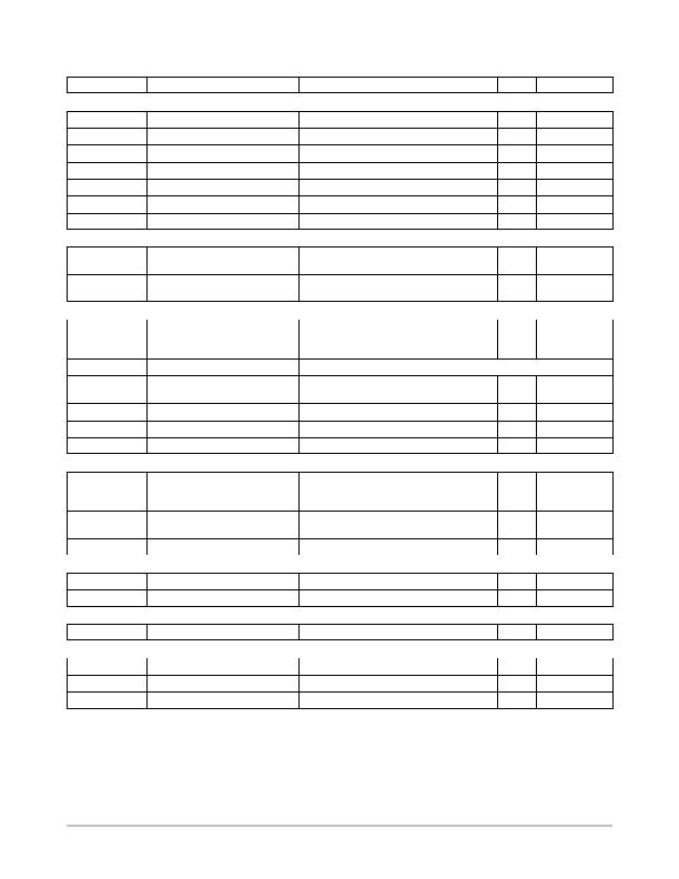
| 型号: | NCP1083DEG |
| 厂商: | ON Semiconductor |
| 文件页数: | 9/18页 |
| 文件大小: | 257K |
| 描述: | IC CONV CTLR POE-PD 40W 20-TSSOP |
| 标准包装: | 74 |
| 类型: | 以太网供电开关(PoE) |
| 应用: | 远程外设(工业控制,相机,数据访问) |
| 内部开关: | 是 |
| 电流限制: | 1.1A |
| 电源电压: | 0 V ~ 57 V |
| 工作温度: | -40°C ~ 85°C |
| 安装类型: | 表面贴装 |
| 封装/外壳: | 20-TSSOP(0.173",4.40mm 宽)裸露焊盘 |
| 供应商设备封装: | 20-TSSOP-EP |
| 包装: | 管件 |
NCP1083
http://onsemi.com
9
Table 3. OPERATING CONDITIONS
Symbol
Parameter
Conditions
Min
Typ
Max
Unit
PASSSWITCH AND CURRENT LIMITS
Ron
Passswitch Rdson
Max Ron specified at Tj = 130癈
0.6
1.2
W
I_Rinrush1
Rinrush = 150 kW (Note 11)
Measured at RTNVPORTN
1,2
= 3 V
95
125
155
mA
I_Rinrush2
Rinrush = 57.6 kW (Note 11)
Measured at RTNVPORTN
1,2
= 3 V
260
310
360
mA
I_Rilim1
Rilim1 = 84.5 kW (Note 11)
Current limit threshold
450
510
570
mA
I_Rilim2
Rilim1 = 66.5 kW (Note 11)
Current limit threshold
600
645
690
mA
I_Rilim3
Rilim1 = 55.6 kW (Note 11)
Current limit threshold
720
770
820
mA
I_Rilim4
Rilim1 = 38.3 kW (Note 11)
Current limit threshold
970
1100
1230
mA
INRUSH AND ILIM1 CURRENT LIMIT TRANSITION
Vds_pgood
VDS required for power good sta-
tus
RTNVPORTN
1,2
falling; voltage
with respect to VPORTN
1,2
0.8
1
1.2
V
Vds_pgood_hyst
VDS hysteresis required for power
good status
Voltage with respect to VPORTN
1,2
8.2
V
VDDH REGULATOR
VDDH_reg
Regulator output voltage
(Notes 12 and 13)
Ivddh_load + Ivddl_load < 10 mA
with Ivddl_load < 2.25 mA and
12.5 V < VPORTP ARTN < 57 V
8.4
9
9.6
V
VDDH_Off
Regulator turnoff voltage
For information only
VDDH_reg + 0.5 V
V
VDDH_lim
VDDH regulator current limit
(Notes 12 and 13)
13
26
mA
VDDH_Por_R
VDDH POR level (rising)
7.3
8.3
V
VDDH_Por_F
VDDH POR level (falling)
6
7
V
VDDH_ovlo
VDDH overvoltage level (rising)
16
18.5
V
VDDL REGULATOR
VDDL_reg
Regulator output voltage
(Notes 12 and 13)
Ivddl_load < 2.25 mA with
Ivddh_load + Ivddl_load < 10 mA and
12.5 V < VPORTP ARTN < 57 V
3.05
3.3
3.55
V
VDDL_Por_R
VDDL POR level (rising)
VDDL
0.2
VDDL
0.02
V
VDDL_Por_F
VDDL POR level (falling)
2.5
2.9
V
GATE DRIVER
Gate_Tr
GATE rise time (1090%)
Cload = 2 nF, VDDHreg = 9 V
50
ns
Gate_Tf
GATE fall time (9010%)
Cload = 2 nF, VDDHreg = 9 V
50
ns
PWM COMPARATOR
VCOMP
COMP control voltage range
For information only
1.3
3
V
ERROR AMPLIFIER
Vbg_fb
Reference voltage
Voltage with respect to ARTN
1.15
1.2
1.25
V
Av_ol
DC open loop gain
For information only
80
dB
GBW
Error amplifier GBW
For information only
1
MHz
11.The current value corresponds to the PoEPD input current (the current flowing in the external Rdet and the quiescent current of the device
are included). Resistors are assumed to have 1% accuracy.
12.Power dissipation must be considered. Load on VDDH and VDDL must be limited especially if VDDH is not powered by an auxiliary winding.
13.Ivddl_load = current flowing out of the VDDL pin.
Ivddh_load = current flowing out of the VDDH pin + current delivered to the Gate Driver (function of the frequency, VDDH voltage & MOSFET
gate capacitance).
相关PDF资料 |
PDF描述 |
|---|---|
| NCP1501DMR2G | IC REG SGL BUCK/LINEAR 8MICRO |
| NCP1578MNR2G | IC REG DL BCK/LINEAR SYNC 20-QFN |
| NCP1601BDR2G | IC PFC CTRL CRM/TRANSITION 8SOIC |
| NCP1603D100R2G | IC CTLR PFC/PWM COMBO 16-SOIC |
| NCP1605DR2G | IC PFC CONTROLLER CCM/DCM 16SOIC |
相关代理商/技术参数 |
参数描述 |
|---|---|
| NCP1083DER2G | 功能描述:DC/DC 开关控制器 POE-PD 40W DC-DC AUX SUPP RoHS:否 制造商:Texas Instruments 输入电压:6 V to 100 V 开关频率: 输出电压:1.215 V to 80 V 输出电流:3.5 A 输出端数量:1 最大工作温度:+ 125 C 安装风格: 封装 / 箱体:CPAK |
| NCP1083QBCGEVB | 功能描述:电源管理IC开发工具 HIGH POWER POE-PD MODULE RoHS:否 制造商:Maxim Integrated 产品:Evaluation Kits 类型:Battery Management 工具用于评估:MAX17710GB 输入电压: 输出电压:1.8 V |
| NCP1083WIRGEVB | 功能描述:电源管理IC开发工具 POE-PD MODULE WITH VAUX RoHS:否 制造商:Maxim Integrated 产品:Evaluation Kits 类型:Battery Management 工具用于评估:MAX17710GB 输入电压: 输出电压:1.8 V |
| NCP1086 | 制造商:ONSEMI 制造商全称:ON Semiconductor 功能描述:1.5 A Adjustable and 3.3 V Fixed Output Linear Regulator |
| NCP1086/D | 制造商:未知厂家 制造商全称:未知厂家 功能描述:1.5 A Adjustable and 3.3 V Fixed Output Linear Regulator |
发布紧急采购,3分钟左右您将得到回复。