- 您现在的位置:买卖IC网 > PDF目录19522 > NCP1280DR2 (ON Semiconductor)IC CTRLR PWM PROG OVP HV 16SOIC PDF资料下载
参数资料
| 型号: | NCP1280DR2 |
| 厂商: | ON Semiconductor |
| 文件页数: | 11/17页 |
| 文件大小: | 0K |
| 描述: | IC CTRLR PWM PROG OVP HV 16SOIC |
| 标准包装: | 2,500 |
| 输出隔离: | 隔离 |
| 频率范围: | 140kHz ~ 320kHz |
| 输入电压: | 7 V ~ 25 V |
| 工作温度: | -40°C ~ 150°C |
| 封装/外壳: | 16-SOIC(0.154",3.90mm 宽) |
| 供应商设备封装: | 16-SOIC N |
| 包装: | 带卷 (TR) |
�� �
�
�NCP1280�
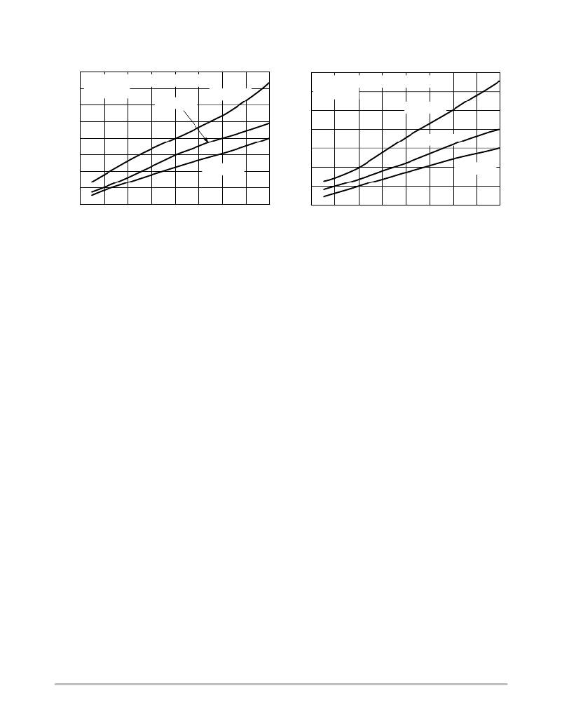
�TYPICAL� CHARACTERISTICS�
�80�
�70�
�60�
�50�
�40�
�30�
�Measured� from� 10%� to� 90%� of� V� OH�
�V� AUX� =� 12� V�
�T� J� =� 25� °� C�
�T� J� = 125� °� C�
�35�
�Measured� from� 90%� to� 10%� of� V� OH�
�30� V� AUX� =� 12� V�
�25� T� J� = 125� °� C�
�20�
�T� J� =� 25� °� C�
�15�
�20�
�10�
�T� J� =� ?� 40� °� C�
�10�
�5�
�T� J� =� ?� 40� °� C�
�0�
�0�
�25�
�50�
�75�
�100�
�125�
�150�
�175�
�200�
�0�
�0�
�25�
�50�
�75�
�100�
�125�
�150�
�175�
�200�
�C� L� ,� LOAD� CAPACITANCE� (pF)�
�Figure� 27.� Outputs� Rise� Time� versus� Load�
�Capacitance�
�C� L� ,� LOAD� CAPACITANCE� (pF)�
�Figure� 28.� Outputs� Fall� Time� versus� Load�
�Capacitance�
�DETAILED� OPERATING� DESCRIPTION�
�Introduction�
�An� NCP1280� based� system� offers� significant� efficiency�
�improvements� and� system� cost� savings� over� a� converter�
�using� a� traditional� forward� topology.� The� NCP1280�
�provides� two� control� outputs.� OUT1� controls� the� primary�
�switch� of� a� forward� converter.� OUT2� has� an� adjustable�
�overlap� delay,� which� can� be� used� to� control� an� active�
�clamp/reset� switch� or� any� other� complementary� drive�
�topology,� such� as� an� asymmetric� half� ?� bridge.� In� addition,�
�OUT2� can� be� used� to� control� a� synchronous� rectifier�
�topology,� eliminating� the� need� of� external� control� circuitry.�
�Other� distinctive� features� include:� two� mode� overcurrent�
�protection,� line� under/overvoltage� detectors,� fast� line�
�feedforward,� soft� ?� start� and� a� maximum� duty� cycle� limit.�
�The� Functional� Block� Diagram� is� shown� in� Figure� 2.�
�The� features� included� in� the� NCP1280� provide� some� of�
�the� advantages� of� Current� ?� Mode� Control,� such� as� fast� line�
�feedforward,� and� cycle� by� cycle� current� limit.� It� eliminates�
�the� disadvantages� of� low� power� jitter,� slope� compensation�
�and� noise� susceptibility.�
�Active� Clamp� Topology�
�The� transformer� reset� voltage� in� a� traditional� forward�
�converter� is� set� by� the� turns� ratio� and� input� voltage.� Where�
�as� the� reset� voltage� of� an� active� clamp� topology� is� constant�
�over� the� converter� off� time� and� only� depends� on� the� input�
�voltage� and� duty� cycle.� This� translates� into� a� lower� voltage�
�stress� on� the� main� switch,� allowing� the� use� of� lower� voltage�
�MOSFETs.� In� general,� lower� voltage� MOSFETs� have� lower�
�High� Voltage� Startup� Regulator�
�The� NCP1280� contains� an� internal� 700� V� startup� regulator�
�that� eliminates� the� need� for� external� startup� components.� In�
�addition,� this� regulator� increases� the� efficiency� of� the� supply�
�as� it� uses� no� power� when� in� the� normal� mode� of� operation,�
�but� instead� uses� power� supplied� by� an� auxiliary� winding.�
�The� startup� regulator� consists� of� a� constant� current� source�
�that� supplies� current� from� the� input� line� voltage� (V� in� )� to� the�
�capacitor� on� the� V� AUX� pin� (C� AUX� ).� The� startup� current� is�
�typically� 13.8� mA.� Once� V� AUX� reaches� 11� V,� the� startup�
�regulator� turns� OFF� and� the� outputs� are� enabled.� When� V� AUX�
�reaches� 7� V,� the� outputs� are� disabled� and� the� startup� regulator�
�turns� ON.� This� “7� ?� 11”� mode� of� operation� is� known� as�
�Dynamic� Self� Supply� (DSS).� The� V� AUX� pin� can� be� biased�
�externally� above� 7� V� once� the� outputs� are� enabled� to� prevent�
�the� startup� regulator� from� turning� ON.� It� is� recommended� to�
�bias� the� V� AUX� pin� using� an� auxiliary� supply� generated� by� an�
�auxiliary� winding� from� the� power� transformer.� An�
�independent� voltage� supply� can� also� be� used.� If� using� an�
�independent� voltage� supply� and� V� AUX� is� biased� before� the�
�outputs� are� enabled� or� while� a� fault� is� present,� the� One� Shot�
�Pulse� Generator� (Figure� 2)� will� not� be� enabled� and� the�
�outputs� will� remain� OFF.�
�As� the� DSS� sources� current� to� the� V� AUX� pin,� a� diode� should�
�be� placed� between� C� AUX� and� the� auxiliary� supply� as� shown�
�in� Figure� 29.� This� will� allow� the� NCP1280� to� charge� C� AUX�
�while� preventing� the� startup� regulator� from� sourcing� current�
�into� the� auxiliary� supply.�
�cost� and� ON� resistance.� Therefore,� lower� system� cost� and�
�higher� efficiency� can� be� achieved.� In� addition,� the� lower�
�voltage� stress� allows� the� converter� to� operate� at� a� higher� duty�
�cycle� for� a� given� primary� switch� voltage� stress.� This� allows�
�a� reduction� in� primary� peak� current� and� secondary� side�
�voltage� stress� as� well� as� smaller� secondary� inductor� size.�
�http://onsemi.com�
�11�
�相关PDF资料 |
PDF描述 |
|---|---|
| TCN75-3.3MOA | IC TEMP SENSOR SRL 3.3V 8SOIC |
| GSA49DTAN | CONN EDGECARD 98POS R/A .125 SLD |
| VE-27J-CY-F4 | CONVERTER MOD DC/DC 36V 50W |
| TC653BEVUATR | IC TEMP SNSR/DC FAN CNTRLR 8MSOP |
| GPM80PG | PS MEDICAL QUAD OUT +5,12,24,-12 |
相关代理商/技术参数 |
参数描述 |
|---|---|
| NCP1280DR2G | 功能描述:电压模式 PWM 控制器 Active Clamp Voltage Mode PWM RoHS:否 制造商:Texas Instruments 输出端数量:1 拓扑结构:Buck 输出电压:34 V 输出电流: 开关频率: 工作电源电压:4.5 V to 5.5 V 电源电流:600 uA 最大工作温度:+ 125 C 最小工作温度:- 40 C 封装 / 箱体:WSON-8 封装:Reel |
| NCP1282 | 制造商:ONSEMI 制造商全称:ON Semiconductor 功能描述:Power Factor Controllers |
| NCP1282BDR2G | 功能描述:电压模式 PWM 控制器 HI PRF RSET PWM CNTR RoHS:否 制造商:Texas Instruments 输出端数量:1 拓扑结构:Buck 输出电压:34 V 输出电流: 开关频率: 工作电源电压:4.5 V to 5.5 V 电源电流:600 uA 最大工作温度:+ 125 C 最小工作温度:- 40 C 封装 / 箱体:WSON-8 封装:Reel |
| NCP1288 | 制造商:ONSEMI 制造商全称:ON Semiconductor 功能描述:Fixed Frequency Current Mode Controller for Flyback Converters |
| NCP1288_11 | 制造商:ONSEMI 制造商全称:ON Semiconductor 功能描述:Fixed Frequency Current Mode Controller for Flyback Converters |
发布紧急采购,3分钟左右您将得到回复。