参数资料
| 型号: | NCP1381DR2G |
| 厂商: | ON Semiconductor |
| 文件页数: | 14/25页 |
| 文件大小: | 0K |
| 描述: | IC REG CTRLR FLYBK ISO CM 14SOIC |
| 标准包装: | 1 |
| PWM 型: | 电流模式 |
| 输出数: | 1 |
| 频率 - 最大: | 125kHz |
| 电源电压: | 11 V ~ 20 V |
| 降压: | 无 |
| 升压: | 无 |
| 回扫: | 是 |
| 反相: | 无 |
| 倍增器: | 无 |
| 除法器: | 无 |
| Cuk: | 无 |
| 隔离: | 是 |
| 工作温度: | 0°C ~ 125°C |
| 封装/外壳: | 14-SOIC(0.154",3.90mm 宽) |
| 包装: | 剪切带 (CT) |
| 其它名称: | NCP1381DR2GOSCT |
�� �
�
�NCP1381,� NCP1382�
�3.2�
�3.1�
�3.0�
�4�
�3�
�2.9�
�2.8�
�2.7�
�2.6�
�Required I� Pmax�
�2�
�1�
�2.5�
�200�
�250�
�300�
�350�
�400�
�0�
�0�
�20�
�40�
�60�
�80�
�100�
�?� ?� Vout� +� VF� +� in� ?�
�Pnc(Vin)� :� =� V� (eq.� 4)�
�V� in� ,� VOLTAGE� (V)�
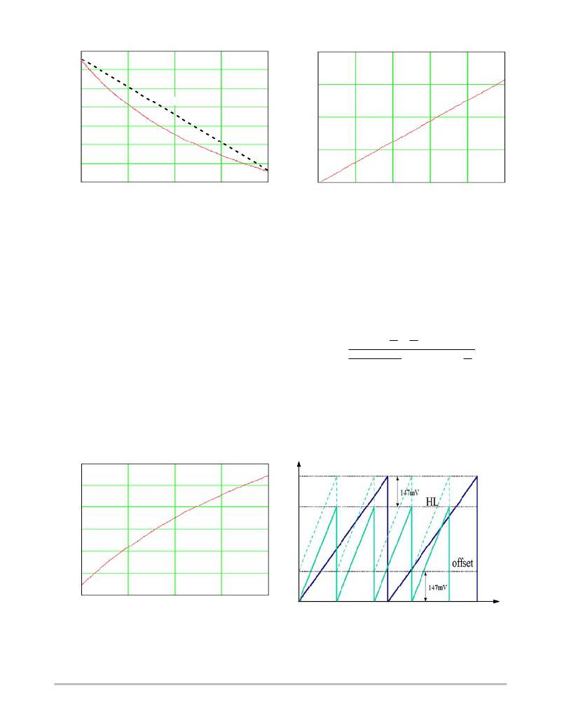
�Figure� 16.� Peak� Current� Evolution� with� Input�
�Voltage� in� a� QR� Converter� at� Constant� Output�
�Power� (100� W)�
�As� a� result,� we� will� probably� calculate� our� sense� resistor�
�to� let� the� converter� bring� the� peak� current� up� to� 3.15� A� at� low�
�mains� (200� VDC� in� follower--boost� configuration).�
�Unfortunately,� in� high� mains� conditions,� where� the� PFC�
�delivers� up� to� 400� VDC,� the� controller� will� also� allow� the�
�same� 3.15� A� maximum� peak� current� (even� a� little� more� with�
�the� propagation� delay)� and� the� power� will� dramatically�
�increase.� In� these� conditions,� the� maximum� power� shall�
�absolutely� be� clamped� in� order� to� avoid� lethal� runaways� in�
�presence� of� a� fault.� If� overpower� compensation� via� a� resistor�
�to� the� bulk� capacitor� offers� a� possible� way,� it� suffers� from� the�
�lack� of� precision� and� good� repeatability� in� production.� It� also�
�degrades� the� standby� consumption.�
�Since� our� controller� integrates� a� brown--out� (BO)�
�protection� that� permanently� senses� the� bulk� capacitor,� we�
�naturally� have� a� voltage� image� of� the� bulk� voltage.� By�
�converting� the� BO� level� into� a� current,� then� routing� this�
�current� in� the� current� sense� (CS)� pin,� we� can� easily� create� a�
�P� O�
�Figure� 17.� I� P� Evolution� with� Output� Power�
�variable� offset� that� will� compensate� the� maximum� output�
�power.� This� would� result� in� a� variable� I� Pmax� as� exemplified�
�by� the� dashed� line� on� Figure� 16.�
�From� the� peak� current� definition,� we� can� extract� the�
�output� power� variation,� with� a� fixed� peak� current� (the�
�maximum� peak� the� controller� will� authorize� is� 0.8� /� R� sense� )�
�and� thus� quantify� the� difference� between� low� and� high� line:�
�R� S� L� P�
�?� 0.8� +� V in� ?� tP� ?�
�2�
�(� η� ?� (Vin� ?� (Vout� +� VF)))� N�
�where�
�t� P� is� the� propagation� delay� (100� ns� typically).�
�If� we� enter� our� previous� parameters� into� the�
�noncompensated� output� power� definition� and� plot� the� result�
�versus� the� input� voltage,� then� we� obtain� the� following� graph,�
�Figure� 18:�
�130�
�125�
�120�
�I� P�
�LL�
�0.8� V�
�0.64� V�
�115�
�110�
�105�
�100�
�200�
�250�
�300�
�350�
�400�
�t�
�V� in� ,� VOLTAGE� (V)�
�Figure� 18.� Output� Power� Evolution� with� the� Input�
�Voltage� (No� Compensation)�
�Figure� 19.� A� Possible� Way� to� Compensate� the�
�Current� Excursion� Lies� in� Offsetting� the�
�Current� Floor�
�http://onsemi.com�
�14�
�相关PDF资料 |
PDF描述 |
|---|---|
| NCP1392BDR2G | IC HALF BRIDGE DVR HV OSC 8SOIC |
| NCP1392DDR2G | IC HALF BRIDGE DVR HV OSC 8SOIC |
| NCP1393BDR2G | IC HALF BRIDGE DVR HV OSC 8SOIC |
| NCP1395BPG | IC REG CTRLR PWM VM 16-DIP |
| NCP1396BDR2G | IC REG CTRLR ISO PWM VM 16-SOIC |
相关代理商/技术参数 |
参数描述 |
|---|---|
| NCP1382DR2G | 功能描述:电流型 PWM 控制器 L-STNDBY PWM CNTRLR RoHS:否 制造商:Texas Instruments 开关频率:27 KHz 上升时间: 下降时间: 工作电源电压:6 V to 15 V 工作电源电流:1.5 mA 输出端数量:1 最大工作温度:+ 105 C 安装风格:SMD/SMT 封装 / 箱体:TSSOP-14 |
| NCP1392B | 制造商:ONSEMI 制造商全称:ON Semiconductor 功能描述:High-Voltage Half-Bridge Driver with Inbuilt Oscillator |
| NCP1392B_09 | 制造商:ONSEMI 制造商全称:ON Semiconductor 功能描述:High-Voltage Half-Bridge Driver with Inbuiltc Oscillator |
| NCP1392BDR2G | 功能描述:功率驱动器IC HV HALF-BRIDGE DRVER RoHS:否 制造商:Micrel 产品:MOSFET Gate Drivers 类型:Low Cost High or Low Side MOSFET Driver 上升时间: 下降时间: 电源电压-最大:30 V 电源电压-最小:2.75 V 电源电流: 最大功率耗散: 最大工作温度:+ 85 C 安装风格:SMD/SMT 封装 / 箱体:SOIC-8 封装:Tube |
| NCP1392DDR2G | 功能描述:功率驱动器IC HV HALF-BRIDGE DRIVER RoHS:否 制造商:Micrel 产品:MOSFET Gate Drivers 类型:Low Cost High or Low Side MOSFET Driver 上升时间: 下降时间: 电源电压-最大:30 V 电源电压-最小:2.75 V 电源电流: 最大功率耗散: 最大工作温度:+ 85 C 安装风格:SMD/SMT 封装 / 箱体:SOIC-8 封装:Tube |
发布紧急采购,3分钟左右您将得到回复。