参数资料
| 型号: | NCP1381DR2G |
| 厂商: | ON Semiconductor |
| 文件页数: | 17/25页 |
| 文件大小: | 0K |
| 描述: | IC REG CTRLR FLYBK ISO CM 14SOIC |
| 标准包装: | 1 |
| PWM 型: | 电流模式 |
| 输出数: | 1 |
| 频率 - 最大: | 125kHz |
| 电源电压: | 11 V ~ 20 V |
| 降压: | 无 |
| 升压: | 无 |
| 回扫: | 是 |
| 反相: | 无 |
| 倍增器: | 无 |
| 除法器: | 无 |
| Cuk: | 无 |
| 隔离: | 是 |
| 工作温度: | 0°C ~ 125°C |
| 封装/外壳: | 14-SOIC(0.154",3.90mm 宽) |
| 包装: | 剪切带 (CT) |
| 其它名称: | NCP1381DR2GOSCT |
�� �
�
�NCP1381,� NCP1382�
�?�
�η� ?� Vin� ?� N� ?� (Vout� +� VF)�
�?�
�?� in� ?� tP�
�is� high,� in� low� power� conditions,� this� voltage� is� low.�
�Unfortunately,� the� situation� complicates� with� QR� converters�
�since� the� input� voltage� plays� a� significant� role� in� the�
�feedback� voltage� evolution.� A� case� can� happen� where� the�
�N� ?� (Vout� +� VF)� +� Vin�
�FB(Vin)� :� =� 2� ?� PO� ?�
�?� RS� ?� FBCS�
�V�
�LP�
�(eq.� 6)�
�?� ?� ?� ?� (eq.� 7)�
�FBComp(Vin)� :� =�
�2� ?� PO� ?�
�?� in� ?� tP]� ?� RS� +� Vin� ?� α� ?� gm� ?� Roffset]�
�converter� is� supplied� by� a� 400� V� rail� and� suddenly� enters�
�standby:� the� PFC� turns� off� and� the� bulk� voltage� goes� low,�
�let’s� say� 120� VDC� (V� in� =� 85� VAC).� At� this� time,� the� power�
�transfer� changes,� the� propagation� delay� plays� a� smaller� role�
�and� the� feedback� voltage� naturally� goes� up� again.� If� a�
�sufficient� hysteresis� is� not� built,� there� are� possibilities� to� see�
�hiccup� on� the� PFC� V� CC� ,� which� is� not� a� desirable� feature.�
�Therefore,� hysteresis� is� mandatory� on� top� of� the�
�Go--To--Standby� (GTS)� detection� level.� For� this� reason� it� is�
�possible� to� increase� the� hysteresis� of� the� ADJ_GTS�
�comparator� due� to� an� internal� 5� m� A� current� source� that� can�
�create� an� offset� to� the� input� signal� if� a� series� resistor� is�
�inserted.� The� ADJ_GTS� detection� level� is� also� adjustable� by�
�tuning� the� portion� of� the� external� signal� applied� to� Pin� 1� (the�
�reference� of� the� internal� comparator� is� 250� mV).�
�Again,� to� check� how� we� manage� the� feedback� variations,�
�we� can� plot� these� variations� without� compensation� for� a�
�given� power,� and� with� the� offset� resistor� connected� to� the� CS�
�pin.� In� the� first� case,� the� FB� voltage� dependency� on� V� in� can�
�be� expressed� by:�
�0.35�
�0.3�
�0.25�
�0.2�
�0.15�
�0.1�
�Where� FB� CS� is� the� ratio� between� the� FB� level� and� the� current�
�setpoint.� In� our� controller,� this� ratio� is� 4.� If� we� now�
�incorporate� our� offset� voltage� generated� by� the� R� offset�
�resistor� and� the� input� voltage,� the� compensated� FB� variation�
�expression� becomes:�
�N� ?� (Vout� +� VF)� +� Vin�
�η� ?� Vin� ?� N� ?� (Vout� ?� VF)�
�V�
�LP�
�?� FBCS�
�with� α� the� BO� divider� ratio� (0.00414� in� our� example),� gm�
�the� transconductance� slope� of� 80� m� S� and� R� offset� ,� the� selected�
�offset� resistor.�
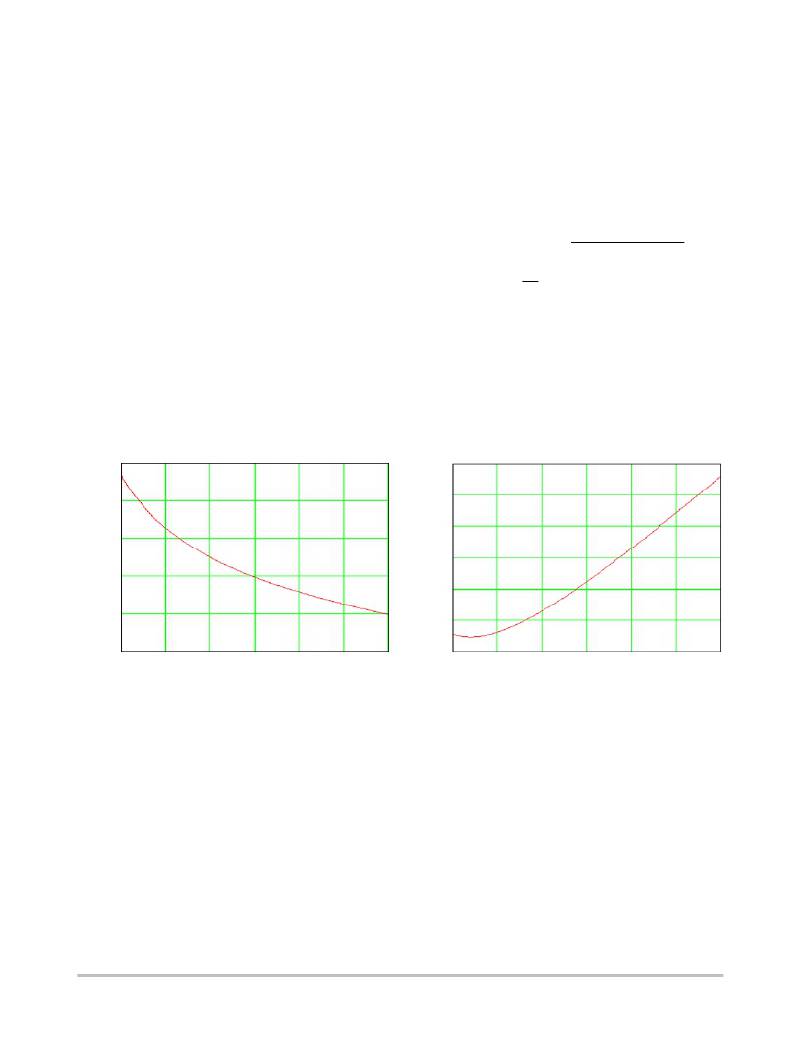
�If� now� plot� Equation� 6� and� Equation� 7� for� a� 8� W� output�
�power,� we� will� obtain� Figures� 25� and� 26:�
�0.75�
�0.7�
�0.65�
�0.6�
�0.55�
�0.5�
�0.45�
�100�
�150�
�200�
�250�
�300�
�350�
�400�
�100�
�150�
�200�
�250�
�300�
�350�
�400�
�0.147� ?� 4� =� 588� mV� <� 0.75� V�
�V� in� ,� VOLTAGE� (V)�
�Figure� 25.� Uncompensated� FB� Variations� for�
�P� out� =� 8� W�
�As� one� can� see� on� Figure� 26,� the� FB� level� now� falls� down�
�when� the� PFC� is� shut� off.� It� now� goes� in� the� right� direction�
�(FB� growing� up� with� V� in� )� and� this� plays� in� our� favor� to� not�
�cross� again� the� upper� comparison� level,� as� it� could� be� the�
�case� in� Figure� 25.� However,� we� must� check� that� the� offset�
�programmed� by� R� offset� (147� mV� in� our� example)� multiplied�
�by� 4,� is� still� below� our� skip� cycle� level,� otherwise� the�
�converter� will� never� enter� skip� at� high� line� (the� permanent�
�offset� at� high� line� will� force� a� higher� feedback):�
�(eq.� 8)�
�This� is� okay.�
�The� drawback� of� Figure� 26� is� the� higher� forced� level� for�
�V� in� ,� VOLTAGE� (V)�
�Figure� 26.� Compensated� FB� variations�
�P� out� =� 8� W�
�PFC� will� be� shutdown� at� P� out� =� 8� W,� or� a� bit� less� than� 10%�
�of� the� nominal� power.� If� the� designer� needs� to� increase� or�
�decrease� this� value,� it� can� adjust� the� ADJ_GTS� level,� still�
�keeping� in� mind� Equation� 8� relationship.�
�To� avoid� a� false� tripping,� the� timer� (90� ms� with� Pin� 4�
�capacitor� of� 220� nF)� will� be� started� every� time� the� GTS�
�signal� goes� high.� If� at� the� end� of� the� 90� ms� the� GTS� signal�
�is� still� high,� the� standby� is� confirmed� and� the� SW� switch�
�between� Pins� 11� and� 10� opens.� To� the� opposite,� when� the�
�output� power� is� needed,� there� is� no� delay� and� the� SW� switch�
�turns� on� immediately.� Figure� 27� zooms� on� the� internal�
�circuitry� whereas� Figure� 28� shows� typical� signal� evolutions:�
�lower� power� outputs.� In� our� example,� a� 90� W� adapter,� the�
�http://onsemi.com�
�17�
�相关PDF资料 |
PDF描述 |
|---|---|
| NCP1392BDR2G | IC HALF BRIDGE DVR HV OSC 8SOIC |
| NCP1392DDR2G | IC HALF BRIDGE DVR HV OSC 8SOIC |
| NCP1393BDR2G | IC HALF BRIDGE DVR HV OSC 8SOIC |
| NCP1395BPG | IC REG CTRLR PWM VM 16-DIP |
| NCP1396BDR2G | IC REG CTRLR ISO PWM VM 16-SOIC |
相关代理商/技术参数 |
参数描述 |
|---|---|
| NCP1382DR2G | 功能描述:电流型 PWM 控制器 L-STNDBY PWM CNTRLR RoHS:否 制造商:Texas Instruments 开关频率:27 KHz 上升时间: 下降时间: 工作电源电压:6 V to 15 V 工作电源电流:1.5 mA 输出端数量:1 最大工作温度:+ 105 C 安装风格:SMD/SMT 封装 / 箱体:TSSOP-14 |
| NCP1392B | 制造商:ONSEMI 制造商全称:ON Semiconductor 功能描述:High-Voltage Half-Bridge Driver with Inbuilt Oscillator |
| NCP1392B_09 | 制造商:ONSEMI 制造商全称:ON Semiconductor 功能描述:High-Voltage Half-Bridge Driver with Inbuiltc Oscillator |
| NCP1392BDR2G | 功能描述:功率驱动器IC HV HALF-BRIDGE DRVER RoHS:否 制造商:Micrel 产品:MOSFET Gate Drivers 类型:Low Cost High or Low Side MOSFET Driver 上升时间: 下降时间: 电源电压-最大:30 V 电源电压-最小:2.75 V 电源电流: 最大功率耗散: 最大工作温度:+ 85 C 安装风格:SMD/SMT 封装 / 箱体:SOIC-8 封装:Tube |
| NCP1392DDR2G | 功能描述:功率驱动器IC HV HALF-BRIDGE DRIVER RoHS:否 制造商:Micrel 产品:MOSFET Gate Drivers 类型:Low Cost High or Low Side MOSFET Driver 上升时间: 下降时间: 电源电压-最大:30 V 电源电压-最小:2.75 V 电源电流: 最大功率耗散: 最大工作温度:+ 85 C 安装风格:SMD/SMT 封装 / 箱体:SOIC-8 封装:Tube |
发布紧急采购,3分钟左右您将得到回复。