- 您现在的位置:买卖IC网 > PDF目录1233 > NCP1631PFCGEVB (ON Semiconductor)BOARD DEMO NCP1631 INTERLEAV PFC PDF资料下载
参数资料
| 型号: | NCP1631PFCGEVB |
| 厂商: | ON Semiconductor |
| 文件页数: | 11/23页 |
| 文件大小: | 0K |
| 描述: | BOARD DEMO NCP1631 INTERLEAV PFC |
| 设计资源: | NCP1631PFCGEVB BOM NCP1631PFCGEVB Gerber Files NCP1631PFCGEVB Schematic |
| 标准包装: | 1 |
| 主要目的: | 电源管理,功率因数校正 |
| 嵌入式: | 否 |
| 已用 IC / 零件: | NCP1631 |
| 已供物品: | 板 |
| 其它名称: | NCP1631PFCGEVBOS |
�� �
�
�NCP1631�
�350,00�
�300,00�
�250,00�
�200,00�
�150,00�
�100,00�
�Vin�
�3,50�
�3,00�
�2,50�
�2,00�
�1,50�
�1,00�
�50,00�
�ton�
�0,50�
�0,00� 0,00�
�0� 2� 4� 6� 8� 10� 12� 14� 16� 18� 20�
�time� (ms)�
�Figure� 8.� Input� Voltage� and� On� ?� time� vs.� Time� (example� with� F� SW� =� 100� kHz,� Pin� =� 150� W,� V� AC� =� 230� V,� L� =� 200� m� H)�
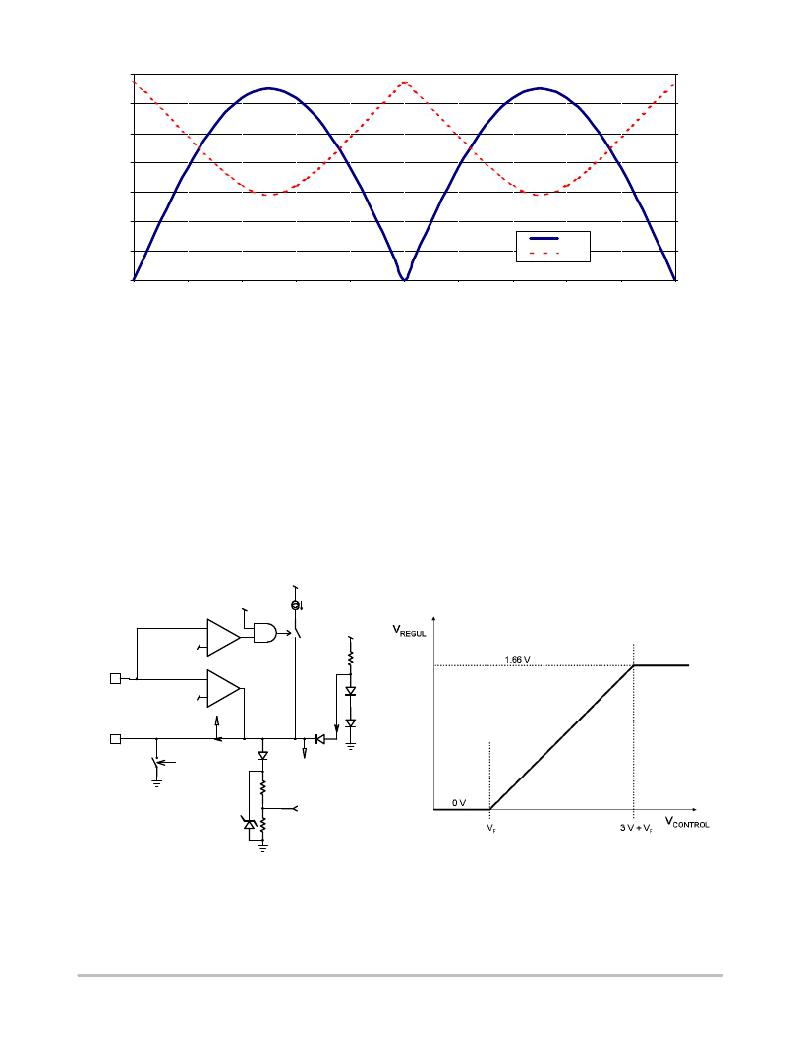
�Regulation� Block� and� Low� Output� Voltage� Detection�
�A� trans� ?� conductance� error� amplifier� with� access� to� the�
�inverting� input� and� output� is� provided.� It� features� a� typical�
�trans� ?� conductance� gain� of� 200� m� S� and� a� typical� capability�
�of� ±� 20� m� A.� The� output� voltage� of� the� PFC� stage� is� typically�
�scaled� down� by� a� resistors� divider� and� monitored� by� the�
�inverting� input� (feed� ?� back� pin� –� pin2).� The� bias� current� is�
�minimized� (less� than� 500� nA)� to� allow� the� use� of� a� high�
�impedance� feed� ?� back� network.� The� output� of� the� error�
�amplifier� is� pinned� out� for� external� loop� compensation�
�(pin5).� Typically� a� type� ?� 2� compensator� is� applied� between�
�pin5� and� ground,� to� set� the� regulation� bandwidth� below�
�20� Hz,� as� need� in� PFC� applications� (refer� to� application�
�note� AND8407).�
�The� swing� of� the� error� amplifier� output� is� limited� within�
�an� accurate� range:�
�?� It� is� forced� above� a� voltage� drop� (V� F� )� by� the� “low�
�clamp”� circuitry.� When� this� circuitry� is� activated,� the�
�power� demand� is� minimum� and� the� NCP1631� enters�
�skip� mode� (the� controller� stops� pulsating)� until� the�
�clamp� is� no� more� active.�
�?� It� is� clamped� not� to� exceed� 3.0� V� +� the� same� V� F�
�voltage� drop.�
�Hence,� V� pin5� features� a� 3� V� voltage� swing.� V� pin5� is� then�
�offset� down� by� (V� F� )� and� further� divided� before� it� connects�
�to� the� “V� ton� processing� block”� and� the� PWM� section.�
�Finally,� the� output� of� the� regulation� is� a� signal� (“V� REGUL� ”�
�of� the� block� diagram)� that� varies� between� 0� and� 1.66� V.�
�Vout� low�
�detect�
�0.955*Vref�
�pfcOK�
�230� m� A�
�VDD�
�FB�
�V� control�
�E� rr� o� r� Am� p� lifier�
�±� 20� m� A�
�Vref�
�OVLflag1�
�OFF�
�5R�
�SKIP� (0� .6� V� c� lamp�
�vo� ltage� is� activated)�
�V� REGUL�
�3V�
�4R�
�Figure� 9.� Regulation� Block�
�http://onsemi.com�
�11�
�Figure� 10.� Correspondence� Between�
�V� CONTROL� and� V� REGUL�
�相关PDF资料 |
PDF描述 |
|---|---|
| NCP1650EVB | BOARD EVAL NCP1650 PFC CTLR |
| NCP1652L48VGEVB | BOARD EVAL 100W 48V NCP1652 PFC |
| NCP1653EVB | BOARD EVAL FOR NCP1653 |
| NCP2993FCT2GEVB | BOARD EVAL NCP2993 AUDIO PWR AMP |
| NCP345SNT1G | IC DETECTOR OVER VOLTAGE 5TSOP |
相关代理商/技术参数 |
参数描述 |
|---|---|
| NCP1650DR2 | 功能描述:功率因数校正 IC Fixed Frequency PFC RoHS:否 制造商:Fairchild Semiconductor 开关频率:300 KHz 最大功率耗散: 最大工作温度:+ 125 C 安装风格:SMD/SMT 封装 / 箱体:SOIC-8 封装:Reel |
| NCP1650DR2G | 功能描述:功率因数校正 IC Fixed Frequency PFC PWM RoHS:否 制造商:Fairchild Semiconductor 开关频率:300 KHz 最大功率耗散: 最大工作温度:+ 125 C 安装风格:SMD/SMT 封装 / 箱体:SOIC-8 封装:Reel |
| NCP1650EVB | 功能描述:电源管理IC开发工具 EVALUATION BOARD RoHS:否 制造商:Maxim Integrated 产品:Evaluation Kits 类型:Battery Management 工具用于评估:MAX17710GB 输入电压: 输出电压:1.8 V |
| NCP1651DR2 | 功能描述:功率因数校正 IC Single Stage PFC RoHS:否 制造商:Fairchild Semiconductor 开关频率:300 KHz 最大功率耗散: 最大工作温度:+ 125 C 安装风格:SMD/SMT 封装 / 箱体:SOIC-8 封装:Reel |
| NCP1651DR2G | 功能描述:功率因数校正 IC Single Stage PFC RoHS:否 制造商:Fairchild Semiconductor 开关频率:300 KHz 最大功率耗散: 最大工作温度:+ 125 C 安装风格:SMD/SMT 封装 / 箱体:SOIC-8 封装:Reel |
发布紧急采购,3分钟左右您将得到回复。