- 您现在的位置:买卖IC网 > PDF目录1233 > NCP1631PFCGEVB (ON Semiconductor)BOARD DEMO NCP1631 INTERLEAV PFC PDF资料下载
参数资料
| 型号: | NCP1631PFCGEVB |
| 厂商: | ON Semiconductor |
| 文件页数: | 17/23页 |
| 文件大小: | 0K |
| 描述: | BOARD DEMO NCP1631 INTERLEAV PFC |
| 设计资源: | NCP1631PFCGEVB BOM NCP1631PFCGEVB Gerber Files NCP1631PFCGEVB Schematic |
| 标准包装: | 1 |
| 主要目的: | 电源管理,功率因数校正 |
| 嵌入式: | 否 |
| 已用 IC / 零件: | NCP1631 |
| 已供物品: | 板 |
| 其它名称: | NCP1631PFCGEVBOS |
�� �
�
�NCP1631�
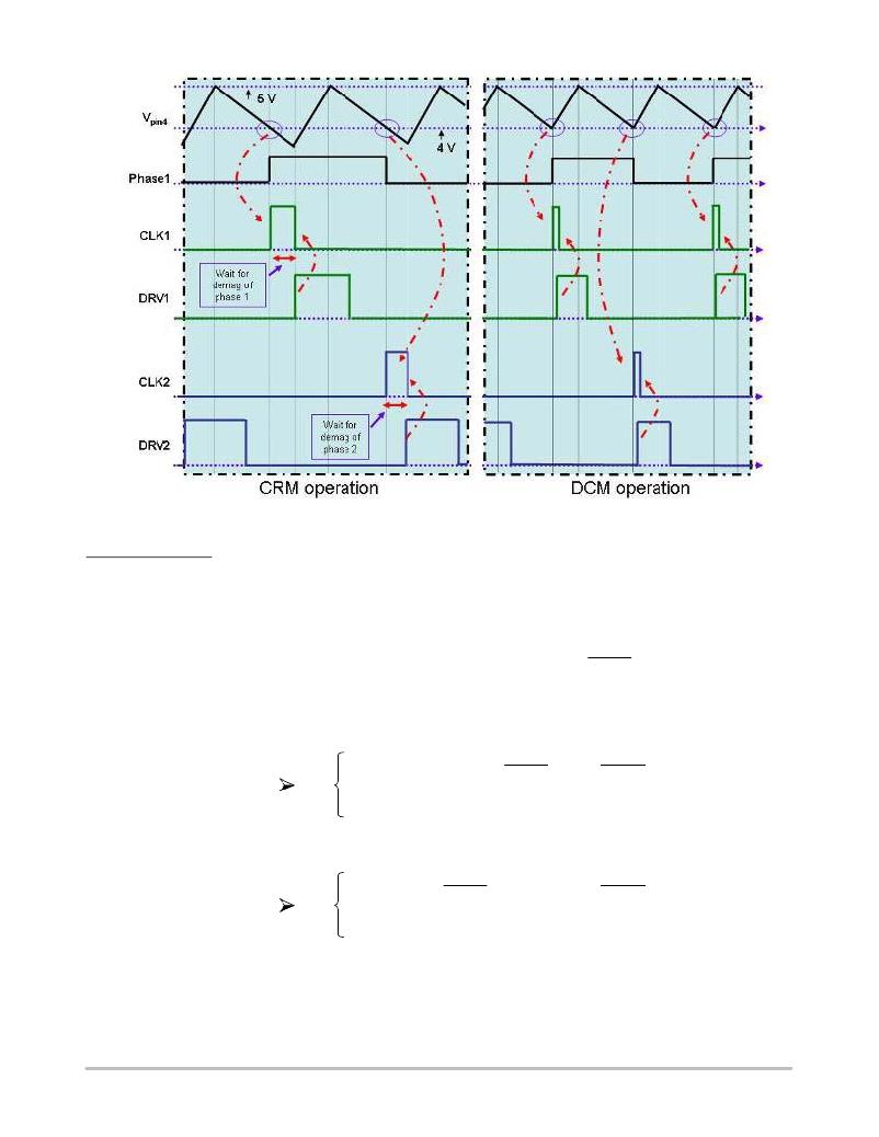
�Figure� 17.� Typical� Waveforms� (T� delay� not� shown� here� for� the� sake� of� simplicity)�
�I� pin6� +� I� FF� +�
�V� REGUL�
�R� FF�
�Frequency Foldback�
�In� addition,� the� circuit� features� the� frequency� fold� ?� back�
�function� to� improve� the� light� load� efficiency.� Practically,�
�the� oscillator� charge� and� discharge� currents� (I� OSC(CH)� and�
�I� OSC(DISCH)� of� Figure� 16)� are� not� constant� but� dependent� on�
�the� power� level.� More� specifically,� I� OSC(CH)� and�
�I� OSC(DISCH)� linearly� vary� as� a� function� of� V� control� output� of�
�the� regulation� block� that� thanks� to� the� feed� ?� forward�
�featured� by� the� NCP1631,� is� representative� of� the� load.�
�The� practical� implementation� is� portrayed� by� Figure� 16.�
�“V� REGUL� ”� is� the� signal� derived� from� V� control� that� is�
�effectively� used� to� modulate� the� MOSFET� on� ?� time.�
�V� REGUL� is� buffered� and� applied� to� pin� 6� (“Frequency�
�fold� ?� back”� pin).� A� resistor� R� FF� is� to� be� connected� to� pin� 6�
�to� sink� a� current� proportional� to� V� REGUL�
�.�
�This� current� is� clamped� not� to� exceed� 105� m� A� and� copied�
�by� a� current� mirror� to� form� I� OSC(CH)� and� I� OSC(DISCH)� .�
�As� a� matter� of� fact,� the� oscillator� charge� current� is:�
�I� OSC(CH)� +� I� OSC(clamp)� )�
�V� REGUL�
�R� FF�
�if�
�V� REGUL�
�R� FF�
�v� 105� m� A�
�(eq.� 18)�
�I� OSC(CH)� +� I� OSC(clamp)� )� I� OSC(CH1)� +� I� OSC(CHT1)� +� 140� m� A�
�The� oscillator� charge� current� is� then� an� increasing� function� of� V� REGUL� and� is� clamped� to� 140� m� A.�
�The� oscillator� discharge� current� is:�
�otherwise�
�I� OSC(DISCH)� +�
�V� REGUL�
�R� FF�
�if�
�V� REGUL�
�R� FF�
�v� 105� m� A�
�(eq.� 19)�
�I� OSC(DISCH)� +� I� OSC(DISCH1)� +� 105� m� A�
�otherwise�
�The� oscillator� discharge� current� is� also� an� increasing�
�function� of� V� REGUL� and� is� clamped� to105� m� A.�
�As� a� consequence,� the� clamp� frequency� is� also� an�
�increasing� function� of� V� REGUL� until� it� reaches� a� maximum�
�value� for� (I� FF� =� 105� m� A).� If� we� consider� the� clamp�
�frequency� f� OSC� computed� by� Equation� 17� as� the� nominal�
�value� obtained� at� full� load� and� if� we� name� it� “f� OSC(nom)� ”:�
�http://onsemi.com�
�17�
�相关PDF资料 |
PDF描述 |
|---|---|
| NCP1650EVB | BOARD EVAL NCP1650 PFC CTLR |
| NCP1652L48VGEVB | BOARD EVAL 100W 48V NCP1652 PFC |
| NCP1653EVB | BOARD EVAL FOR NCP1653 |
| NCP2993FCT2GEVB | BOARD EVAL NCP2993 AUDIO PWR AMP |
| NCP345SNT1G | IC DETECTOR OVER VOLTAGE 5TSOP |
相关代理商/技术参数 |
参数描述 |
|---|---|
| NCP1650DR2 | 功能描述:功率因数校正 IC Fixed Frequency PFC RoHS:否 制造商:Fairchild Semiconductor 开关频率:300 KHz 最大功率耗散: 最大工作温度:+ 125 C 安装风格:SMD/SMT 封装 / 箱体:SOIC-8 封装:Reel |
| NCP1650DR2G | 功能描述:功率因数校正 IC Fixed Frequency PFC PWM RoHS:否 制造商:Fairchild Semiconductor 开关频率:300 KHz 最大功率耗散: 最大工作温度:+ 125 C 安装风格:SMD/SMT 封装 / 箱体:SOIC-8 封装:Reel |
| NCP1650EVB | 功能描述:电源管理IC开发工具 EVALUATION BOARD RoHS:否 制造商:Maxim Integrated 产品:Evaluation Kits 类型:Battery Management 工具用于评估:MAX17710GB 输入电压: 输出电压:1.8 V |
| NCP1651DR2 | 功能描述:功率因数校正 IC Single Stage PFC RoHS:否 制造商:Fairchild Semiconductor 开关频率:300 KHz 最大功率耗散: 最大工作温度:+ 125 C 安装风格:SMD/SMT 封装 / 箱体:SOIC-8 封装:Reel |
| NCP1651DR2G | 功能描述:功率因数校正 IC Single Stage PFC RoHS:否 制造商:Fairchild Semiconductor 开关频率:300 KHz 最大功率耗散: 最大工作温度:+ 125 C 安装风格:SMD/SMT 封装 / 箱体:SOIC-8 封装:Reel |
发布紧急采购,3分钟左右您将得到回复。