- 您现在的位置:买卖IC网 > PDF目录22207 > NCP1650DR2 (ON Semiconductor)IC CTRLR PWR FACTOR PWM 16SOIC PDF资料下载
参数资料
| 型号: | NCP1650DR2 |
| 厂商: | ON Semiconductor |
| 文件页数: | 28/31页 |
| 文件大小: | 0K |
| 描述: | IC CTRLR PWR FACTOR PWM 16SOIC |
| 标准包装: | 1 |
| 模式: | 连续导电(CCM),间歇导电(DCM) |
| 频率 - 开关: | 100kHz |
| 电源电压: | 10 V ~ 20 V |
| 工作温度: | -40°C ~ 125°C |
| 安装类型: | 表面贴装 |
| 封装/外壳: | 16-SOIC(0.154",3.90mm 宽) |
| 供应商设备封装: | 16-SOIC |
| 包装: | 标准包装 |
| 其它名称: | NCP1650DR2OSDKR |
第1页第2页第3页第4页第5页第6页第7页第8页第9页第10页第11页第12页第13页第14页第15页第16页第17页第18页第19页第20页第21页第22页第23页第24页第25页第26页第27页当前第28页第29页第30页第31页
�� �
�
�NCP1650�
�in� the� introduction� to� this� analysis,� this� is� not� analyzed�
�separately.�
�The� equation� for� the� gain� is� good� for� frequencies� below�
�the� pole.� There� is� a� single� pole� due� to� the� output� filter.� Since�
�the� NCP1650� is� a� current� mode� converter,� the� inductor� is� not�
�part� of� the� output� pole� as� can� be� seen� in� that� equation.�
�Plot� the� sum� of� these� three� values.� Figure� 43� shows� a� gain�
�of� 35.5� dB� until� the� pole� of� the� output� filter� is� reached� at�
�0.3� Hz.� After� that,� the� gain� is� reduced� at� a� rate� of�
�20� dB/decade.�
�40�
�Calculating� the� Loop� Gain�
�At� this� point� in� the� design� process,� all� of� the� parameters�
�involved� in� this� calculation� have� been� determined� with� the�
�exception� of� the� pole--zero� pair� on� the� output� of� the� voltage�
�error� amplifier.�
�All� equations� give� gains� in� absolute� numbers.� It� is�
�necessary� to� convert� these� to� the� decibel� format� using� the�
�following� formula:�
�30�
�20�
�10�
�0�
�--10�
�--20�
�LOOP� GAIN�
�WITHOUT�
�ERROR� AMP�
�A� =�
�=� .0099�
�A(dB)� =� 20� Log10� (A)�
�For� example,� the� voltage� divider� would� be:�
�5.6� k�
�560� k� +� 5.6� k�
�--30�
�--40�
�0.01�
�0.1�
�1� 10�
�FREQUENCY� (Hz)�
�100�
�1000�
�C� =�
�=� 85� m� F�
�A(dB)� =� 20� Log10� .0099� =� ?� 40� dB�
�The� gain� of� the� loop� will� vary� as� the� input� voltage� changes.�
�It� is� recommended� that� the� compensation� for� the� voltage�
�error� amplifier� be� calculated� under� high� line,� full� load�
�conditions.� This� should� be� the� greatest� bandwidth� that� the�
�unit� will� see.�
�By� necessity,� the� unity� gain� (OdB)� loop� bandwidth� for� a�
�PFC� unit,� must� be� less� than� the� line� frequency.� If� the�
�bandwidth� approaches� or� exceeds� the� line� frequency,� the�
�voltage� error� amplifier� signal� will� have� frequency�
�components� in� its� output� that� are� greater� than� the� line�
�frequency.� These� components� will� cause� distortion� in� the�
�output� of� the� reference� amplifier,� which� is� used� to� shape� the�
�current� waveform.� This� in� turn� will� cause� distortion� in� the�
�current� and� reduce� the� power� factor.�
�Typically� the� maximum� bandwidth� for� a� 60� Hz� PFC�
�converter� is� 10� Hz,� and� slightly� less� for� a� 50� Hz� system.� This�
�can� be� adjusted� to� meet� the� particular� requirements� of� a�
�system.� The� unity� gain� bandwidth� is� determined� by� the�
�frequency� at� which� the� loop� gain� passes� through� the� 0� dB�
�level.�
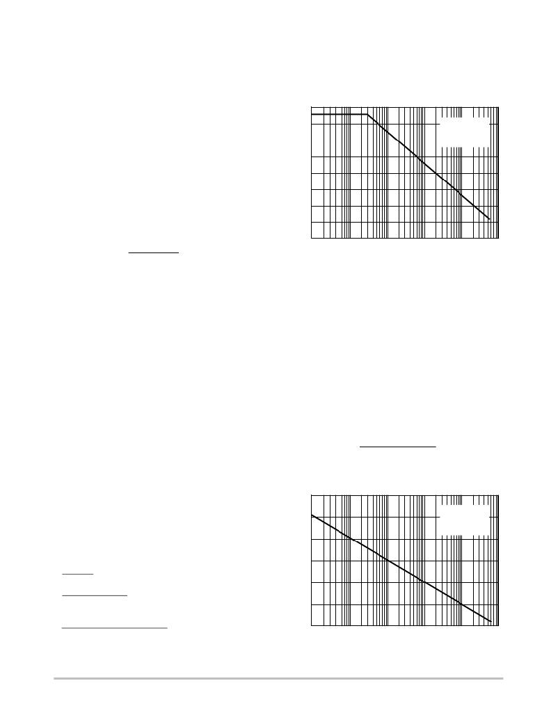
�Figure� 43.� Open� Loop� Gain� Less� Error� Amp�
�A� typical� error� amplifier� bode� plot� is� shown� in� Figure� 44.�
�The� zero� is� used� to� offset� the� pole� of� the� output� filter.� The�
�output� filter� pole� will� typically� be� lower� than� the� unity� gain�
�loop� bandwidth,� so� the� zero� will� be� necessary.�
�This� plot� shows� a� forward� gain� of� 7.0� dB� at� 10� Hz.� To�
�compensate� for� this� the� error� amplifier� should� have� a� gain� of�
�–7.0� dB� (0.45)� at� 10� Hz,� and� a� zero� at� 0.4� Hz.� The� gain� at�
�10� Hz� is� determined� by� the� resistor� since� it� is� well� past� the�
�zero.� The� resistor� can� be� calculated� by� the� equation:�
�R7� =� Av� ∕� Gm� =� .45� ∕� .0001� =� 4.5� k� Ω�
�4.7� kW� is� the� closest� standard� value.� Using� this,� the�
�capacitor� can� be� calculated� based� on� the� zero� frequency� of�
�0.4� Hz.� This� would� give� a� value� for� C� 7� of:�
�1�
�2� ?� π� ?� 4.7� k� ?� 0.4� Hz�
�Using� these� values� (4.7� k� Ω� and� 86� m� F),� the� open� loop� gain�
�plot� would� be:�
�80�
�For� stability� purposes,� the� gain� should� pass� through� 0� dB�
�with� a� slope� of� –20� dB/decade� for� approximately� one� decade�
�on� either� side� of� the� unity� gain� frequency.� This� assures� a�
�phase� margin� of� greater� than� 45� ?� .�
�The� gain� can� be� calculated� graphically� using� the� equations�
�of� Figure� 43� as� follows:�
�Divider:� Calculate� V’/Vo� in� dB,� this� value� is� constant� so�
�it� will� not� change� with� frequency.�
�Reference Signal:� Calculate� V� ref� /V� e/a� using� the� peak� level�
�of� the� AC� input� signal� at� high� line� that� will� be� seen� on� pin� 5.�
�Convert� this� to� dB.� This� is� also� a� constant� value.�
�60�
�40�
�20�
�0�
�--20�
�VOLTAGE�
�LOOP� BODE�
�PLOT�
�Modulator and Output Stage:� Calculate� the� gain� in� dB� for�
�DVo/DVref.� Calculate� the� pole� frequency.� The� gain� will� be�
�constant� for� all� frequencies� less� than� f� p� .� Starting� at� the� pole�
�frequency,� this� gain� will� drop� off� at� a� rate� of� 20� dB/decade.�
�--40�
�0.01� 0.1� 1� 10� 100�
�FREQUENCY� (Hz)�
�Figure� 44.� Open� Loop� Gain� of� Voltage� Loop�
�1000�
�http://onsemi.com�
�28�
�相关PDF资料 |
PDF描述 |
|---|---|
| KA78RM33RTM | IC REG LDO 3.3V .5A DPAK |
| RJZ-2412S/H | CONV DC/DC 2W 24VIN 12VOUT |
| VE-J0Y-IZ | CONVERTER MOD DC/DC 3.3V 16.5W |
| HSC26DRYI-S93 | CONN EDGECARD 52POS DIP .100 SLD |
| NCP1601AP | IC CTRLR PFC FREQ DCM/CRM 8DIP |
相关代理商/技术参数 |
参数描述 |
|---|---|
| NCP1650DR2G | 功能描述:功率因数校正 IC Fixed Frequency PFC PWM RoHS:否 制造商:Fairchild Semiconductor 开关频率:300 KHz 最大功率耗散: 最大工作温度:+ 125 C 安装风格:SMD/SMT 封装 / 箱体:SOIC-8 封装:Reel |
| NCP1650EVB | 功能描述:电源管理IC开发工具 EVALUATION BOARD RoHS:否 制造商:Maxim Integrated 产品:Evaluation Kits 类型:Battery Management 工具用于评估:MAX17710GB 输入电压: 输出电压:1.8 V |
| NCP1651DR2 | 功能描述:功率因数校正 IC Single Stage PFC RoHS:否 制造商:Fairchild Semiconductor 开关频率:300 KHz 最大功率耗散: 最大工作温度:+ 125 C 安装风格:SMD/SMT 封装 / 箱体:SOIC-8 封装:Reel |
| NCP1651DR2G | 功能描述:功率因数校正 IC Single Stage PFC RoHS:否 制造商:Fairchild Semiconductor 开关频率:300 KHz 最大功率耗散: 最大工作温度:+ 125 C 安装风格:SMD/SMT 封装 / 箱体:SOIC-8 封装:Reel |
| NCP1652ADR2G | 功能描述:功率因数校正 IC ANA PFC CONTROLLER RoHS:否 制造商:Fairchild Semiconductor 开关频率:300 KHz 最大功率耗散: 最大工作温度:+ 125 C 安装风格:SMD/SMT 封装 / 箱体:SOIC-8 封装:Reel |
发布紧急采购,3分钟左右您将得到回复。