- 您现在的位置:买卖IC网 > PDF目录22207 > NCP1650DR2 (ON Semiconductor)IC CTRLR PWR FACTOR PWM 16SOIC PDF资料下载
参数资料
| 型号: | NCP1650DR2 |
| 厂商: | ON Semiconductor |
| 文件页数: | 3/31页 |
| 文件大小: | 0K |
| 描述: | IC CTRLR PWR FACTOR PWM 16SOIC |
| 标准包装: | 1 |
| 模式: | 连续导电(CCM),间歇导电(DCM) |
| 频率 - 开关: | 100kHz |
| 电源电压: | 10 V ~ 20 V |
| 工作温度: | -40°C ~ 125°C |
| 安装类型: | 表面贴装 |
| 封装/外壳: | 16-SOIC(0.154",3.90mm 宽) |
| 供应商设备封装: | 16-SOIC |
| 包装: | 标准包装 |
| 其它名称: | NCP1650DR2OSDKR |
第1页第2页当前第3页第4页第5页第6页第7页第8页第9页第10页第11页第12页第13页第14页第15页第16页第17页第18页第19页第20页第21页第22页第23页第24页第25页第26页第27页第28页第29页第30页第31页
�� �
�
�NCP1650�
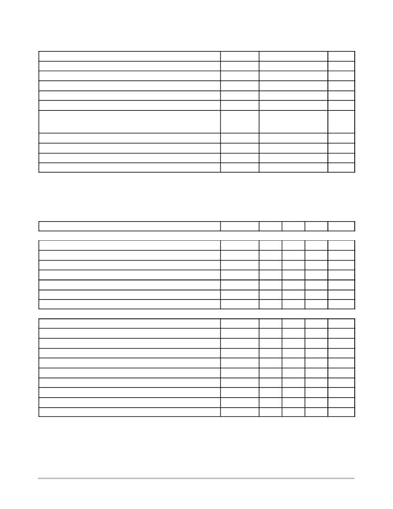
�MAXIMUM� RATINGS� (Maximum� ratings� are� those� that,� if� exceeded,� may� cause� damage� to� the� device.� Electrical� Characteristics� are�
�not� guaranteed� over� this� range.)�
�Rating�
�Power� Supply� Voltage� (Operating)� Output� (Pin� 16)�
�Current� Sense� Inverting� Input� (Pin� 12)�
�Reference� Voltage� (Pin� 2)�
�Reference� Filter� (Pin� 4)�
�All� Other� Inputs�
�Thermal� Resistance,� Junction--to--Air�
�0.1� in� 2� Copper�
�0.5� in� 2� Copper�
�Thermal� Resistance,� Junction--to--Lead� (Pin� 1)� (Note� 1)�
�Maximum� Power� Dissipation� @� T� A� =� 25� ?� C�
�Operating� Temperature� Range�
�Non--operating� Temperature� Range�
�Symbol�
�V� CC�
�V(I� S� --)�
�V� ref�
�Ref� fltr�
�θ� JA�
�θ� JL�
�P� max�
�T� J�
�T� J�
�Value�
�--0.3� to� 20�
�--0.5� to� 1.0�
�--0.3� to� 7.5�
�--0.3� to� 5.0�
�--0.3� to� 6.5�
�130�
�110�
�50�
�0.77�
�--40� to� 125�
�--55� to� 150�
�Unit�
�V�
�V�
�V�
�V�
�V�
�?� C/W�
�?� C/W�
�W�
�?� C�
�?� C�
�Stresses� exceeding� Maximum� Ratings� may� damage� the� device.� Maximum� Ratings� are� stress� ratings� only.� Functional� operation� above� the�
�Recommended� Operating� Conditions� is� not� implied.� Extended� exposure� to� stresses� above� the� Recommended� Operating� Conditions� may� affect�
�device� reliability.�
�1.� θ� JL� is� equivalent� to� Psi� JL�
�ELECTRICAL� CHARACTERISTICS� (Unless� otherwise� noted:� V� CC� =� 14� volts,� C� T� =� 470� pF,� C� 2� =� 0.1� m� F,� T� J� =� 25� ?� C� for� typical�
�values.� For� min/max� values� T� J� is� the� applicable� junction� temperature.)�
�Characteristic�
�Symbol�
�Min�
�Typ�
�Max�
�Unit�
�OSCILLATOR�
�Frequency�
�Max� Duty� Cycle�
�Min� Duty� Cycle� (Note� 2)�
�Ramp� Peak� (Note� 2)�
�Ramp� Valley� (Note� 2)�
�Ramp� Compensation� Peak� Voltage� (Pin� 13)� (Note� 2)�
�Ramp� Compensation� Current� (Pin� 13)� (Note� 2)�
�F� osc�
�dmax�
�dmin�
�V� Rpeak�
�V� Rvalley�
�--�
�--�
�90�
�0.95�
�--�
�--�
�--�
�--�
�--�
�100�
�0.97�
�0�
�4.0�
�0.100�
�4.0�
�400�
�110�
�--�
�5.0�
�--�
�--�
�--�
�--�
�kHz�
�--�
�%�
�V�
�V�
�V�
�m� A�
�VOLTAGE� ERROR� AMPLIFIER�
�Input� Bias� Current� (Note� 2)�
�Input� Offset� Voltage� (Note� 2)�
�Transconductance� (T� J� =� --40� ?� C� to� +� 125� ?� C)�
�Output� Source� (V� ref� +� 0.2� V)�
�Output� Sink� (V� ref� --� 0.2� V)�
�I� bias�
�V� IO�
�g� m�
�I� Osource�
�I� Osink�
�--�
�--�
�90�
�10�
�--10�
�0.2�
�10�
�120�
�20�
�--20�
�0.6�
�--�
�150�
�--�
�--�
�m� A�
�mV�
�umho�
�m� A�
�m� A�
�Boost� Current� (V� ref� =� 4.0� volts� nominal)�
�Source� Boost� Current� Threshold� (V� pin6� /V� ref� )�
�Sink� Boost� Current� Threshold� (V� pin6� /V� ref� )�
�Source� Boost� Current� (V� ref� +� 0.4� V)�
�Sink� Boost� Current� (V� ref� --� 0.4� V)�
�V� fb(boost+)�
�V� fb(boost--)�
�I� (boost+)�
�I� (boost--)�
�--�
�--�
�150�
�--150�
�1.06�
�0.920�
�230�
�--260�
�--�
�--�
�--�
�--�
�V/V�
�V/V�
�m� A�
�m� A�
�2.� Verified� by� design.�
�http://onsemi.com�
�3�
�相关PDF资料 |
PDF描述 |
|---|---|
| KA78RM33RTM | IC REG LDO 3.3V .5A DPAK |
| RJZ-2412S/H | CONV DC/DC 2W 24VIN 12VOUT |
| VE-J0Y-IZ | CONVERTER MOD DC/DC 3.3V 16.5W |
| HSC26DRYI-S93 | CONN EDGECARD 52POS DIP .100 SLD |
| NCP1601AP | IC CTRLR PFC FREQ DCM/CRM 8DIP |
相关代理商/技术参数 |
参数描述 |
|---|---|
| NCP1650DR2G | 功能描述:功率因数校正 IC Fixed Frequency PFC PWM RoHS:否 制造商:Fairchild Semiconductor 开关频率:300 KHz 最大功率耗散: 最大工作温度:+ 125 C 安装风格:SMD/SMT 封装 / 箱体:SOIC-8 封装:Reel |
| NCP1650EVB | 功能描述:电源管理IC开发工具 EVALUATION BOARD RoHS:否 制造商:Maxim Integrated 产品:Evaluation Kits 类型:Battery Management 工具用于评估:MAX17710GB 输入电压: 输出电压:1.8 V |
| NCP1651DR2 | 功能描述:功率因数校正 IC Single Stage PFC RoHS:否 制造商:Fairchild Semiconductor 开关频率:300 KHz 最大功率耗散: 最大工作温度:+ 125 C 安装风格:SMD/SMT 封装 / 箱体:SOIC-8 封装:Reel |
| NCP1651DR2G | 功能描述:功率因数校正 IC Single Stage PFC RoHS:否 制造商:Fairchild Semiconductor 开关频率:300 KHz 最大功率耗散: 最大工作温度:+ 125 C 安装风格:SMD/SMT 封装 / 箱体:SOIC-8 封装:Reel |
| NCP1652ADR2G | 功能描述:功率因数校正 IC ANA PFC CONTROLLER RoHS:否 制造商:Fairchild Semiconductor 开关频率:300 KHz 最大功率耗散: 最大工作温度:+ 125 C 安装风格:SMD/SMT 封装 / 箱体:SOIC-8 封装:Reel |
发布紧急采购,3分钟左右您将得到回复。