- 您现在的位置:买卖IC网 > PDF目录1233 > NCP1652L48VGEVB (ON Semiconductor)BOARD EVAL 100W 48V NCP1652 PFC PDF资料下载
参数资料
| 型号: | NCP1652L48VGEVB |
| 厂商: | ON Semiconductor |
| 文件页数: | 27/34页 |
| 文件大小: | 0K |
| 描述: | BOARD EVAL 100W 48V NCP1652 PFC |
| 产品变化通告: | 1Q2012 Discontinuation 30/Mar/2012 |
| 标准包装: | 1 |
| 系列: | * |
| 其它名称: | NCP1652L48VGEVB-ND NCP1652L48VGEVBOS |
第1页第2页第3页第4页第5页第6页第7页第8页第9页第10页第11页第12页第13页第14页第15页第16页第17页第18页第19页第20页第21页第22页第23页第24页第25页第26页当前第27页第28页第29页第30页第31页第32页第33页第34页
�� �
�
�NCP1652,� NCP1652A�
�Output� Overload�
�The� Feedback� Voltage,� V� FB� ,� is� directly� proportional� to� the�
�output� power� of� the� converter.� An� internal� 6.7� k� W� resistor�
�pulls� ?� up� the� FB� voltage� to� the� internal� 6.5� V� reference.� An�
�external� optocoupler� pulls� down� the� FB� voltage� to� regulate�
�the� output� voltage� of� the� system.� The� optocoupler� is� off�
�during� power� up� and� output� overload� conditions� allowing�
�the� FB� voltage� to� reach� its� maximum� level.�
�The� NCP1652� monitors� the� FB� voltage� to� detect� an�
�overload� condition.� A� typical� startup� time� of� a� single� PFC�
�stage� converter� is� around� 100� ms.� If� the� converter� is� out� of�
�regulation� (FB� voltage� exceeds� 5.0� V)� for� more� that� 150� ms�
�(typical)� the� drivers� are� disabled� and� the� controller� enters� the�
�double� hiccup� mode� to� reduce� the� average� power�
�dissipation.� A� new� startup� sequence� is� initiated� after� the�
�double� hiccup� is� complete.� This� protection� feature� is� critical�
�to� reduce� power� during� an� output� short� condition.�
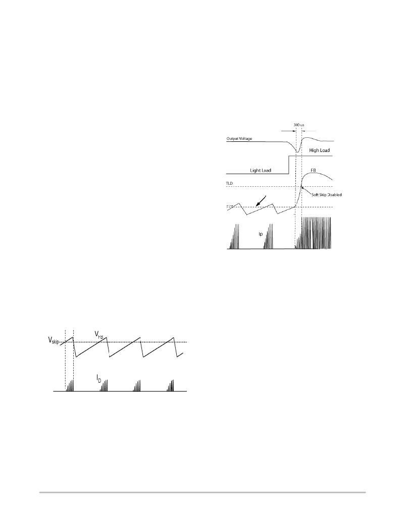
�Soft� ?� Skip� ?� Cycle� Mode�
�The� FB� voltage� reduces� as� the� output� power� demand� of� the�
�260� mV.� A� new� Soft� ?� Skip� ?� period� starts� once� the� voltage�
�on� the� AC� ?� IN� pin� increases� to� 260� mV.�
�An� increase� in� output� load� current� terminates� a�
�Soft� ?� Skip� ?� event.� A� transient� load� detector� terminates� a�
�Soft� ?� Skip� ?� period� once� V� FB� voltage� exceeds� V� SSKIP� by�
�more� than� 550� mV.� This� ensures� the� required� output� power�
�is� delivered� during� a� load� transient� and� the� output� voltage�
�does� not� fall� out� of� regulation.� Figure� 66� shows� the�
�relationship� between� Soft� ?� Skip� ?� and� the� transient� load�
�detector.�
�converter� reduces.� Once� V� FB� drops� below� the� skip�
�threshold,� V� SSKIP� ,� 1.30� V� (typical)� the� drivers� are� disabled.�
�The� skip� comparator� hysteresis� is� typically� 180� mV.�
�The� converter� output� voltage� starts� to� decay� because� no�
�additional� output� power� is� delivered.� As� the� output� voltage�
�decreases� the� feedback� voltage� increases� to� maintain� the�
�output� voltage� in� regulation.� This� mode� of� operation� is�
�known� as� skip� mode.� The� skip� mode� frequency� is� dependent�
�V� FB�
�V� SSKIP�
�of� load� loop� gain� and� output� capacitance� and� can� create�
�audible� noise� due� to� mechanical� resonance� in� the�
�transformer� and� snubber� capacitor.� A� proprietary�
�Soft� ?� Skip� ?� mode� reduces� audible� noise� by� slowly�
�increasing� the� primary� peak� current� until� it� reaches� its�
�maximum� value.� The� minimum� skip� ramp� period,� t� SSKIP� ,� is�
�2.5� ms.� Figure� 65� shows� the� relationship� between� V� FB� ,�
�V� SSKIP� and� the� primary� current.�
�Figure� 65.� Soft� ?� Skip� ]� operation.�
�Skip� mode� operation� is� synchronous� of� the� ac� line� voltage.�
�The� NCP1652� disables� Soft� ?� Skip� ?� when� the� rectified� ac�
�line� voltage� drops� to� its� valley� level.� This� ensures� the�
�primary� current� always� ramp� up� reducing� audible� noise.� A�
�skip� event� occurring� as� the� ac� line� voltage� is� decreasing,�
�causes� the� primary� peak� current� to� ramp� down� instead� of�
�ramp� up.� Once� the� skip� period� is� over� the� primary� current� is�
�only� determined� by� the� ac� line� voltage.� A� Soft� ?� Skip� ?� event�
�terminates� once� the� AC� ?� IN� pin� voltage� decreases� below�
�Figure� 66.� Load� transient� during� Soft� ?� Skip� ]�
�The� output� of� the� Soft� ?� Skip� ?� Comparator� is� or� ?� ed� with�
�the� PWM� Comparator� output� to� control� the� duty� ratio.� The�
�Soft� ?� Skip� ?� Comparator� controls� the� duty� ratio� in� skip�
�mode� and� the� PWM� Comparator� controls� the� duty� cycle�
�during� normal� operation.� In� skip� mode,� the� non� ?� inverting�
�input� of� the� Soft� ?� Skip� ?� Comparator� exceeds� 4� V,� disabling�
�the� drivers.� As� the� FB� voltage� increases,� the� voltage� at� the�
�non� ?� inverting� input� is� ramp� down� from� 4� V� to� 0.2� V� to�
�enable� the� drivers.�
�Multiplier� and� Reference� Generator�
�The� NCP1652� uses� a� multiplier� to� regulate� the� average�
�output� power� of� the� converter.� This� controller� uses� a�
�proprietary� concept� for� the� multiplier� used� within� the�
�reference� generator.� This� innovative� design� allows� greatly�
�improved� accuracy� compared� to� a� conventional� linear�
�analog� multiplier.� The� multiplier� uses� a� PWM� switching�
�circuit� to� create� a� scalable� output� signal,� with� a� very� well�
�defined� gain.�
�The� output� of� the� multiplier� is� the� ac-reference� signal.� The�
�ac-reference� signal� is� used� to� shape� the� input� current.� The�
�multiplier� has� three� inputs,� the� error� signal� from� an� external�
�error� amplifier� (V� FB� ),� the� full� wave� rectified� ac� input�
�(AC_IN)� and� the� feedforward� input� (V� FF� ).�
�The� FB� signal� from� an� external� error� amplifier� circuit� is�
�applied� to� the� V� FB� pin� via� an� optocoupler� or� other� isolation�
�circuit.� The� FB� voltage� is� converted� to� a� current� with� a� V-I�
�http://onsemi.com�
�27�
�相关PDF资料 |
PDF描述 |
|---|---|
| NCP1653EVB | BOARD EVAL FOR NCP1653 |
| NCP2993FCT2GEVB | BOARD EVAL NCP2993 AUDIO PWR AMP |
| NCP345SNT1G | IC DETECTOR OVER VOLTAGE 5TSOP |
| NCP346SN2T1G | IC DETECTOR OVER VOLTAGE 5TSOP |
| NCP347MTAITBG | IC OVERVOLTAGE PROT CTRLR 10WDFN |
相关代理商/技术参数 |
参数描述 |
|---|---|
| NCP1653ADR2 | 功能描述:功率因数校正 IC Fixed Frequency RoHS:否 制造商:Fairchild Semiconductor 开关频率:300 KHz 最大功率耗散: 最大工作温度:+ 125 C 安装风格:SMD/SMT 封装 / 箱体:SOIC-8 封装:Reel |
| NCP1653ADR2G | 功能描述:功率因数校正 IC Fixed Frequency Current Mode PFC RoHS:否 制造商:Fairchild Semiconductor 开关频率:300 KHz 最大功率耗散: 最大工作温度:+ 125 C 安装风格:SMD/SMT 封装 / 箱体:SOIC-8 封装:Reel |
| NCP1653ADR2G-CUT TAPE | 制造商:ON 功能描述:NCP1653 Series 15 V 6 mA Current-Mode Power Factor Correction Controller SOIC-8 |
| NCP1653AP | 功能描述:功率因数校正 IC Fixed Frequency RoHS:否 制造商:Fairchild Semiconductor 开关频率:300 KHz 最大功率耗散: 最大工作温度:+ 125 C 安装风格:SMD/SMT 封装 / 箱体:SOIC-8 封装:Reel |
| NCP1653APG | 功能描述:功率因数校正 IC Fixed Frequency Current Mode PFC RoHS:否 制造商:Fairchild Semiconductor 开关频率:300 KHz 最大功率耗散: 最大工作温度:+ 125 C 安装风格:SMD/SMT 封装 / 箱体:SOIC-8 封装:Reel |
发布紧急采购,3分钟左右您将得到回复。