- 您现在的位置:买卖IC网 > PDF目录1233 > NCP1652L48VGEVB (ON Semiconductor)BOARD EVAL 100W 48V NCP1652 PFC PDF资料下载
参数资料
| 型号: | NCP1652L48VGEVB |
| 厂商: | ON Semiconductor |
| 文件页数: | 28/34页 |
| 文件大小: | 0K |
| 描述: | BOARD EVAL 100W 48V NCP1652 PFC |
| 产品变化通告: | 1Q2012 Discontinuation 30/Mar/2012 |
| 标准包装: | 1 |
| 系列: | * |
| 其它名称: | NCP1652L48VGEVB-ND NCP1652L48VGEVBOS |
第1页第2页第3页第4页第5页第6页第7页第8页第9页第10页第11页第12页第13页第14页第15页第16页第17页第18页第19页第20页第21页第22页第23页第24页第25页第26页第27页当前第28页第29页第30页第31页第32页第33页第34页
�� �
�
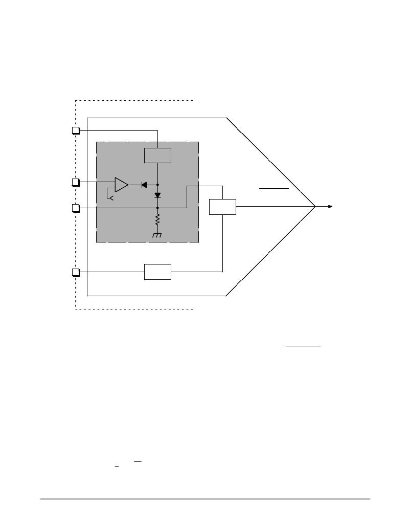
�NCP1652,� NCP1652A�
�converter.� There� is� no� error� in� the� output� signal� due� to� the�
�series� rectifier� as� shown� in� Figure� 67.�
�The� scaled� version� of� the� full� wave� rectified� input� ac� wave�
�is� applied� to� the� AC_IN� pin� by� means� of� a� resistive� voltage�
�divider.� The� multiplier� ramp� is� generated� by� comparing� the�
�scaled� line� voltage� to� the� oscillator� ramp� with� the� AC_IN�
�Comparator.� The� current� signal� from� the� V-I� converter� is�
�FB�
�Multiplier�
�V� ?� to� ?� I�
�factored� by� the� AC_IN� comparator� output.� The� resulting�
�signal� is� filtered� by� the� low� pass� R-C� filter� on� the� CM� pin.�
�The� low� pass� filter� removes� the� high� frequency� content.� The�
�gain� of� the� multiplier� is� determined� by� the� V-I� converter,� the�
�resistor� on� the� CM� pin,� and� the� peak� and� valley� voltages� of�
�the� oscillator� sawtooth� ramp.�
�FB�
�AC_IN�
�AC� IN�
�+�
�?�
�Oscillator�
�V�
�AC_REF�
�+� k� @�
�V�
�@� V�
�FF�
�V� 2�
�CM�
�Divide�
�AC_REF�
�V� FF�
�Square�
�V� FF2�
�Figure� 67.� Reference� Generator�
�V� AC_REF� +� @� k� (eq.� 8)�
�V� FF�
�V� FF� +�
�Vac� 2� a�
�The� third� input� to� the� reference� generator� is� the� V� FF� signal.�
�The� V� FF� signal� is� a� dc� voltage� proportional� to� the� ac� line�
�voltage.� A� resistive� voltage� divider� attenuates� the� full� wave�
�rectified� line� voltage� between� 0.7� and� 5.0� V.� The� full� wave�
�rectified� line� is� then� averaged� with� a� capacitor.� The� ac�
�average� voltage� must� be� constant� over� each� half� cycle� of� the�
�line.� Line� voltage� ripple� (120� Hz� or� 100� Hz)� ripple� on� the�
�V� FF� signal� adds� ripple� to� the� output� of� the� multiplier.� This�
�will� distort� the� ac� reference� signal� and� reduce� the� power�
�factor� and� increase� the� line� current� distortion.� Excessive�
�filtering� delays� the� feedforward� signal� reducing� the� line�
�transient� response.� A� good� starting� point� is� to� set� the� filter�
�time� constant� to� one� cycle� of� the� line� voltage.� The� user� can�
�then� optimize� the� filter� for� line� transient� response� versus�
�power� factor.� The� average� voltage� on� the� V� FF� pin� is:�
�2�
�p� (eq.� 7)�
�Where,� a� is� the� voltage� divider� ratio,� normally� 0.01.�
�V� FB� @� V� AC_IN�
�2�
�The� multiplier� transfer� function� is� given� by� Equation� 8.�
�The� output� of� the� multiplier� is� the� AC_REF.� It� connects� to�
�the� AC� Error� Amplifier.�
�where,� k� is� the� reference� generator� gain,� typically� 0.55.� The�
�output� of� the� reference� generator� is� clamped� at� 4.5� V� to� limit�
�the� maximum� output� power.�
�Feedforward� maintains� a� constant� input� power�
�independent� of� the� line� voltage.� That� is,� for� a� given� FB�
�voltage,� if� the� line� voltage� doubles� (AC_IN),� the�
�feedforward� term� quadruples� and� reduces� the� output� of� the�
�error� amplifier� in� half� to� maintain� the� same� input� power.�
�AC� Error� Amplifier� Compensation�
�A� pole-zero� pair� is� created� by� placing� a� series� combination�
�of� R� COMP� and� C� COMP� at� the� output� of� the� AC� error� amplifier�
�(EA).� The� value� of� the� compensation� components� is�
�http://onsemi.com�
�28�
�相关PDF资料 |
PDF描述 |
|---|---|
| NCP1653EVB | BOARD EVAL FOR NCP1653 |
| NCP2993FCT2GEVB | BOARD EVAL NCP2993 AUDIO PWR AMP |
| NCP345SNT1G | IC DETECTOR OVER VOLTAGE 5TSOP |
| NCP346SN2T1G | IC DETECTOR OVER VOLTAGE 5TSOP |
| NCP347MTAITBG | IC OVERVOLTAGE PROT CTRLR 10WDFN |
相关代理商/技术参数 |
参数描述 |
|---|---|
| NCP1653ADR2 | 功能描述:功率因数校正 IC Fixed Frequency RoHS:否 制造商:Fairchild Semiconductor 开关频率:300 KHz 最大功率耗散: 最大工作温度:+ 125 C 安装风格:SMD/SMT 封装 / 箱体:SOIC-8 封装:Reel |
| NCP1653ADR2G | 功能描述:功率因数校正 IC Fixed Frequency Current Mode PFC RoHS:否 制造商:Fairchild Semiconductor 开关频率:300 KHz 最大功率耗散: 最大工作温度:+ 125 C 安装风格:SMD/SMT 封装 / 箱体:SOIC-8 封装:Reel |
| NCP1653ADR2G-CUT TAPE | 制造商:ON 功能描述:NCP1653 Series 15 V 6 mA Current-Mode Power Factor Correction Controller SOIC-8 |
| NCP1653AP | 功能描述:功率因数校正 IC Fixed Frequency RoHS:否 制造商:Fairchild Semiconductor 开关频率:300 KHz 最大功率耗散: 最大工作温度:+ 125 C 安装风格:SMD/SMT 封装 / 箱体:SOIC-8 封装:Reel |
| NCP1653APG | 功能描述:功率因数校正 IC Fixed Frequency Current Mode PFC RoHS:否 制造商:Fairchild Semiconductor 开关频率:300 KHz 最大功率耗散: 最大工作温度:+ 125 C 安装风格:SMD/SMT 封装 / 箱体:SOIC-8 封装:Reel |
发布紧急采购,3分钟左右您将得到回复。