- 您现在的位置:买卖IC网 > PDF目录1233 > NCP1652L48VGEVB (ON Semiconductor)BOARD EVAL 100W 48V NCP1652 PFC PDF资料下载
参数资料
| 型号: | NCP1652L48VGEVB |
| 厂商: | ON Semiconductor |
| 文件页数: | 4/34页 |
| 文件大小: | 0K |
| 描述: | BOARD EVAL 100W 48V NCP1652 PFC |
| 产品变化通告: | 1Q2012 Discontinuation 30/Mar/2012 |
| 标准包装: | 1 |
| 系列: | * |
| 其它名称: | NCP1652L48VGEVB-ND NCP1652L48VGEVBOS |
第1页第2页第3页当前第4页第5页第6页第7页第8页第9页第10页第11页第12页第13页第14页第15页第16页第17页第18页第19页第20页第21页第22页第23页第24页第25页第26页第27页第28页第29页第30页第31页第32页第33页第34页
�� �
�
�NCP1652,� NCP1652A�
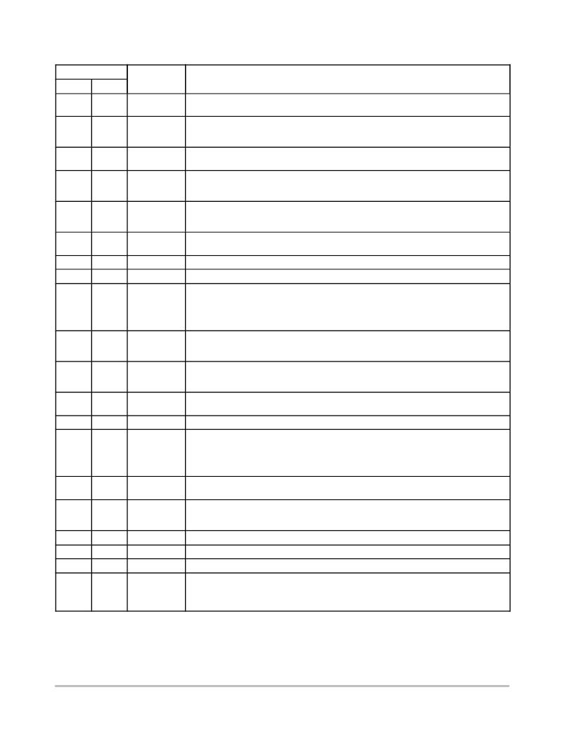
�PIN� FUNCTION� DESCRIPTION�
�Pin�
�16� Pin�
�1�
�2�
�3�
�4�
�5�
�6�
�7�
�8�
�9�
�10�
�11�
�12�
�13�
�14�
�15�
�16�
�20� Pin�
�1�
�2�
�3�
�4�
�5�
�6�
�7�
�8�
�9�
�10�
�11�
�12�
�13�
�14�
�15�
�16�
�17�
�18�
�19�
�20�
�Symbol�
�C� T�
�RAMP� COMP�
�AC� IN�
�FB�
�VFF�
�CM�
�NC�
�NC�
�AC� COMP�
�Latch�
�Rdelay�
�I� AVG�
�I� Spos�
�V� CC�
�OUTA�
�OUTB�
�GND�
�NC�
�NC�
�HV�
�Description�
�An� external� timing� capacitor� (C� T� )� sets� the� oscillator� frequency.� A� sawtooth� between� 0.2� V� and� 4�
�V� sets� the� oscillator� frequency� and� the� gain� of� the� multiplier.�
�A� resistor� (R� RC� )� between� this� pin� and� ground� adjust� the� amount� of� ramp� compensation� that� is�
�added� to� the� current� signal.� Ramp� compensation� is� required� to� prevent� subharmonic� oscilla-�
�tions.� This� pin� should� not� be� left� open.�
�The� scaled� version� of� the� full� wave� rectified� input� ac� wave� is� connected� to� this� pin� by� means� of�
�a� resistive� voltage� divider.� The� line� voltage� information� is� used� by� the� multiplier.�
�An� error� signal� from� an� external� error� amplifier� circuit� is� fed� to� this� pin� via� an� optocoupler� or�
�other� isolation� circuit.� The� FB� voltage� is� a� proportional� of� the� load� of� the� converter.� If� the� voltage�
�on� the� FB� pin� drops� below� V� SSKIP� the� controller� enters� Soft� ?� Skip� ?� to� reduce� acoustic� noise.�
�Feedforward� input.� A� scaled� version� of� the� filtered� rectified� line� voltage� is� applied� by� means� of� a�
�resistive� divider� and� an� averaging� capacitor.� The� information� is� used� by� the� Reference� Generat-�
�or� to� regulate� the� controller.�
�Multiplier� output.� A� capacitor� is� connected� between� this� pin� and� ground� to� filter� the� modulated�
�output� of� the� multiplier.�
�Sets� the� pole� for� the� ac� reference� amplifier.� The� reference� amplifier� compares� the� low� fre-�
�quency� component� of� the� input� current� to� the� ac� reference� signal.� The� response� must� be� slow�
�enough� to� filter� out� most� of� the� high� frequency� content� of� the� current� signal� that� is� injected� from�
�the� current� sense� amplifier,� but� fast� enough� to� cause� minimal� distortion� to� the� line� frequency�
�information.� The� pin� should� not� be� left� open.�
�Latch� ?� Off� input.� Pulling� this� pin� below� 1.0� V� (typical)� or� pulling� it� above� 7.0� V� (typical)� latches�
�the� controller.� This� input� can� be� used� to� implement� an� overvoltage� detector,� an� overtemperature�
�detector� or� both.� Refer� to� Figure� 69� for� a� typical� implementation.�
�A� resistor� between� this� pin� and� ground� sets� the� non� ?� overlap� time� delay� between� OUTA� and�
�OUTB.� The� delay� is� adjusted� to� prevent� cross� conduction� between� the� primary� MOSFET� and�
�synchronous� rectification� MOSFET� or� optimize� the� resonant� transition� in� an� active� clamp� stage.�
�An� external� resistor� and� capacitor� connected� from� this� terminal� to� ground,� to� set� and� stabilizes�
�the� gain� of� the� current� sense� amplifier� output� that� drives� the� ac� error� amplifier.�
�Positive� current� sense� input.� Connects� to� the� positive� side� of� the� current� sense� resistor.�
�Positive� input� supply.� This� pin� connects� to� an� external� capacitor� for� energy� storage.� An� internal�
�current� source� supplies� current� from� the� STARTUP� pin� V� CC� .� Once� the� voltage� on� V� CC� reaches�
�approximately� 15.3� V,� the� current� source� turns� off� and� the� outputs� are� enabled.� The� drivers� are�
�disabled� once� V� CC� reaches� approximately� 10.3� V.� If� V� CC� drops� below� 0.85� V� (typical),� the� star-�
�tup� current� is� reduced� to� less� than� 500� m� A.�
�Drive� output� for� the� main� flyback� power� MOSFET� or� IGBT.� OUTA� has� a� source� resistance� of�
�13� W� (typical)� and� a� sink� resistance� of� 8� W� (typical).�
�Secondary� output� of� the� PWM� Controller.� It� can� be� used� to� drive� synchronous� rectifier,� and�
�active� clamp� switch,� or� both.� OUTB� has� source� and� sink� resistances� of� 22� W� (typical)� and� 11�
�(typical),� respectively.�
�Ground� reference� for� the� circuit.�
�Connect� the� rectified� input� line� voltage� directly� to� this� pin� to� enable� the� internal� startup� regulator.�
�A� constant� current� source� supplies� current� from� this� pin� to� the� capacitor� connected� to� the� V� CC�
�pin,� eliminating� the� need� for� a� startup� resistor.� The� charge� current� is� typically� 5.5� mA.� Maximum�
�input� voltage� is� 500� V.�
�http://onsemi.com�
�4�
�相关PDF资料 |
PDF描述 |
|---|---|
| NCP1653EVB | BOARD EVAL FOR NCP1653 |
| NCP2993FCT2GEVB | BOARD EVAL NCP2993 AUDIO PWR AMP |
| NCP345SNT1G | IC DETECTOR OVER VOLTAGE 5TSOP |
| NCP346SN2T1G | IC DETECTOR OVER VOLTAGE 5TSOP |
| NCP347MTAITBG | IC OVERVOLTAGE PROT CTRLR 10WDFN |
相关代理商/技术参数 |
参数描述 |
|---|---|
| NCP1653ADR2 | 功能描述:功率因数校正 IC Fixed Frequency RoHS:否 制造商:Fairchild Semiconductor 开关频率:300 KHz 最大功率耗散: 最大工作温度:+ 125 C 安装风格:SMD/SMT 封装 / 箱体:SOIC-8 封装:Reel |
| NCP1653ADR2G | 功能描述:功率因数校正 IC Fixed Frequency Current Mode PFC RoHS:否 制造商:Fairchild Semiconductor 开关频率:300 KHz 最大功率耗散: 最大工作温度:+ 125 C 安装风格:SMD/SMT 封装 / 箱体:SOIC-8 封装:Reel |
| NCP1653ADR2G-CUT TAPE | 制造商:ON 功能描述:NCP1653 Series 15 V 6 mA Current-Mode Power Factor Correction Controller SOIC-8 |
| NCP1653AP | 功能描述:功率因数校正 IC Fixed Frequency RoHS:否 制造商:Fairchild Semiconductor 开关频率:300 KHz 最大功率耗散: 最大工作温度:+ 125 C 安装风格:SMD/SMT 封装 / 箱体:SOIC-8 封装:Reel |
| NCP1653APG | 功能描述:功率因数校正 IC Fixed Frequency Current Mode PFC RoHS:否 制造商:Fairchild Semiconductor 开关频率:300 KHz 最大功率耗散: 最大工作温度:+ 125 C 安装风格:SMD/SMT 封装 / 箱体:SOIC-8 封装:Reel |
发布紧急采购,3分钟左右您将得到回复。