- 您现在的位置:买卖IC网 > PDF目录15521 > NCP3011DTBR2G (ON Semiconductor)IC REG CTRLR BUCK PWM VM 14TSSOP PDF资料下载
参数资料
| 型号: | NCP3011DTBR2G |
| 厂商: | ON Semiconductor |
| 文件页数: | 24/28页 |
| 文件大小: | 0K |
| 描述: | IC REG CTRLR BUCK PWM VM 14TSSOP |
| 标准包装: | 1 |
| PWM 型: | 电压模式 |
| 输出数: | 1 |
| 频率 - 最大: | 470kHz |
| 占空比: | 83% |
| 电源电压: | 4.7 V ~ 28 V |
| 降压: | 是 |
| 升压: | 无 |
| 回扫: | 无 |
| 反相: | 无 |
| 倍增器: | 无 |
| 除法器: | 无 |
| Cuk: | 无 |
| 隔离: | 无 |
| 工作温度: | -40°C ~ 125°C |
| 封装/外壳: | 14-TSSOP(0.173",4.40mm 宽) |
| 包装: | 标准包装 |
| 其它名称: | NCP3011DTBR2GOSDKR |
第1页第2页第3页第4页第5页第6页第7页第8页第9页第10页第11页第12页第13页第14页第15页第16页第17页第18页第19页第20页第21页第22页第23页当前第24页第25页第26页第27页第28页
�� �
�
�NCP3011,� NCV3011�
�I� G1�
�I� G2�
�where:�
�Q� GD� Q� GD�
�t� ON� +� +� (eq.� 32)�
�V� BST� *� V� TH� R� HSPU� )� R� G�
�and:�
�Q� GD� Q� GD�
�t� OFF� +� +� (eq.� 33)�
�V� BST� *� V� TH� R� HSPD� )� R� G�
�Next,� the� MOSFET� output� capacitance� losses� are� caused�
�by� both� the� control� and� synchronous� MOSFET� but� are�
�dissipated� only� in� the� control� MOSFET.�
�2�
�P� DS� +� 1� @� Q� OSS� @� V� IN� @� f� SW� (eq.� 34)�
�Finally� the� loss� due� to� the� reverse� recovery� time� of� the�
�body� diode� in� the� synchronous� MOSFET� is� shown� as�
�follows:�
�P� RR� +� Q� RR� @� V� IN� @� f� SW� (eq.� 35)�
�The� low� ?� side� or� synchronous� MOSFET� turns� on� into� zero�
�volts� so� switching� losses� are� negligible.� Its� power�
�dissipation� only� consists� of� conduction� loss� due� to� R� DS(on)�
�and� body� diode� loss� during� the� non� ?� overlap� periods.�
�P� D_SYNC� +� P� COND� )� P� BODY� (eq.� 36)�
�Conduction� loss� in� the� low� ?� side� or� synchronous�
�MOSFET� is� described� as� follows:�
�2�
�P� COND� +� I� RMS_SYNC� @� R� DS(on)_SYNC� (eq.� 37)�
�I� G1� :� output� current� from� the� high� ?� side� gate� drive� (HSDR)�
�I� G2� :� output� current� from� the� low� ?� side� gate� drive� (LSDR)�
�?� SW� :� switching� frequency� of� the� converter.�
�V� BST� :� gate� drive� voltage� for� the� high� ?� side� drive,� typically�
�7.5� V.�
�Q� GD� :� gate� charge� plateau� region,� commonly� specified� in� the�
�MOSFET� datasheet�
�V� TH� :� gate� ?� to� ?� source� voltage� at� the� gate� charge� plateau�
�region�
�Q� OSS� :� MOSFET� output� gate� charge� specified� in� the� data�
�sheet�
�Q� RR� :� reverse� recovery� charge� of� the� low� ?� side� or�
�synchronous� MOSFET,� specified� in� the� datasheet�
�R� DS(on)_CONTROL� :� on� resistance� of� the� high� ?� side,� or�
�control,� MOSFET�
�R� DS(on)_SYNC� :� on� resistance� of� the� low� ?� side,� or�
�synchronous,� MOSFET�
�NOL� LH� :� dead� time� between� the� LSDR� turning� off� and� the�
�HSDR� turning� on,� typically� 85� ns�
�NOL� HL� :� dead� time� between� the� HSDR� turning� off� and� the�
�LSDR� turning� on,� typically� 75� ns�
�Once� the� MOSFET� power� dissipations� are� determined,�
�the� designer� can� calculate� the� required� thermal� impedance�
�for� each� device� to� maintain� a� specified� junction� temperature�
�at� the� worst� case� ambient� temperature.� The� formula� for�
�calculating� the� junction� temperature� with� the� package� in� free�
�air� is:�
�(� 1� *� D)� @� 1� )�
�I� RMS_SYNC� +� I� OUT� @�
�where:�
�ra� 2�
�12�
�The� body� diode� losses� can� be� approximated� as:�
�P� BODY� +� V� FD� @� I� OUT� @� f� SW� @� NOL� LH� )� NOL� HL�
�Vth�
�(eq.� 38)�
�(eq.� 39)�
�T� J� +� T� A� )� P� D� @� R� q� JA�
�T� J� :� Junction� Temperature�
�T� A� :� Ambient� Temperature�
�P� D� :� Power� Dissipation� of� the� MOSFET� under� analysis�
�R� q� JA� :� Thermal� Resistance� Junction� ?� to� ?� Ambient� of� the�
�MOSFET’s� package�
�As� with� any� power� design,� proper� laboratory� testing�
�should� be� performed� to� insure� the� design� will� dissipate� the�
�required� power� under� worst� case� operating� conditions.�
�Variables� considered� during� testing� should� include�
�maximum� ambient� temperature,� minimum� airflow,�
�maximum� input� voltage,� maximum� loading,� and� component�
�variations� (i.e.� worst� case� MOSFET� R� DS(on)� ).�
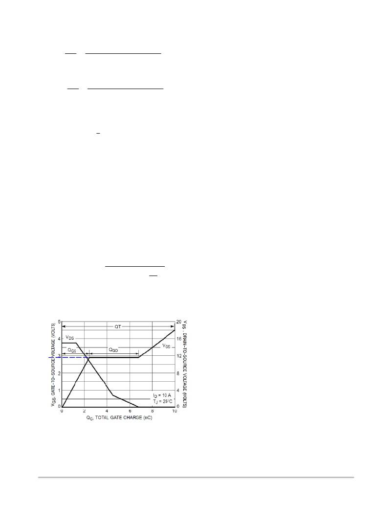
�Figure� 43.� MOSFET� Switching� Characteristics�
�http://onsemi.com�
�24�
�相关PDF资料 |
PDF描述 |
|---|---|
| RPP50-483.3S | CONV DC/DC 50W 36-75VIN 3.3VOUT |
| RPP40-2424DW | CONV DC/DC 40W 9-36V +/-24VOUT |
| RPP40-2415DW-F | CONV DC/DC 40W 9-36V +/-15VOUT |
| RPP40-2415DW-1F | CONV DC/DC 40W 9-36V +/-15VOUT |
| RPP40-2415DW-1 | CONV DC/DC 40W 9-36V +/-15VOUT |
相关代理商/技术参数 |
参数描述 |
|---|---|
| NCP3011GEVB | 功能描述:电源管理IC开发工具 NCP3011 EVALUATION BOARD RoHS:否 制造商:Maxim Integrated 产品:Evaluation Kits 类型:Battery Management 工具用于评估:MAX17710GB 输入电压: 输出电压:1.8 V |
| NCP3012 | 制造商:ONSEMI 制造商全称:ON Semiconductor 功能描述:Synchronous PWM Controller |
| NCP3012DTBR2G | 功能描述:电压模式 PWM 控制器 Single Output Buck 0.8V to 40V 70uA RoHS:否 制造商:Texas Instruments 输出端数量:1 拓扑结构:Buck 输出电压:34 V 输出电流: 开关频率: 工作电源电压:4.5 V to 5.5 V 电源电流:600 uA 最大工作温度:+ 125 C 最小工作温度:- 40 C 封装 / 箱体:WSON-8 封装:Reel |
| NCP301HSN09T1 | 功能描述:电压监测器/监控器 0.9V Detector RoHS:否 制造商:Texas Instruments 监测电压数:2 监测电压:Adjustable 输出类型:Open Drain 欠电压阈值: 过电压阈值: 准确性:1 % 工作电源电压:1.5 V to 6.5 V 工作电源电流:1.8 uA 最大工作温度:+ 125 C 封装 / 箱体:SON-6 安装风格:SMD/SMT |
| NCP301HSN09T1G | 功能描述:电压监测器/监控器 0.9V Detector w/Reset High RoHS:否 制造商:Texas Instruments 监测电压数:2 监测电压:Adjustable 输出类型:Open Drain 欠电压阈值: 过电压阈值: 准确性:1 % 工作电源电压:1.5 V to 6.5 V 工作电源电流:1.8 uA 最大工作温度:+ 125 C 封装 / 箱体:SON-6 安装风格:SMD/SMT |
发布紧急采购,3分钟左右您将得到回复。