- 您现在的位置:买卖IC网 > PDF目录15521 > NCP3011DTBR2G (ON Semiconductor)IC REG CTRLR BUCK PWM VM 14TSSOP PDF资料下载
参数资料
| 型号: | NCP3011DTBR2G |
| 厂商: | ON Semiconductor |
| 文件页数: | 26/28页 |
| 文件大小: | 0K |
| 描述: | IC REG CTRLR BUCK PWM VM 14TSSOP |
| 标准包装: | 1 |
| PWM 型: | 电压模式 |
| 输出数: | 1 |
| 频率 - 最大: | 470kHz |
| 占空比: | 83% |
| 电源电压: | 4.7 V ~ 28 V |
| 降压: | 是 |
| 升压: | 无 |
| 回扫: | 无 |
| 反相: | 无 |
| 倍增器: | 无 |
| 除法器: | 无 |
| Cuk: | 无 |
| 隔离: | 无 |
| 工作温度: | -40°C ~ 125°C |
| 封装/外壳: | 14-TSSOP(0.173",4.40mm 宽) |
| 包装: | 标准包装 |
| 其它名称: | NCP3011DTBR2GOSDKR |
第1页第2页第3页第4页第5页第6页第7页第8页第9页第10页第11页第12页第13页第14页第15页第16页第17页第18页第19页第20页第21页第22页第23页第24页第25页当前第26页第27页第28页
�� �
�
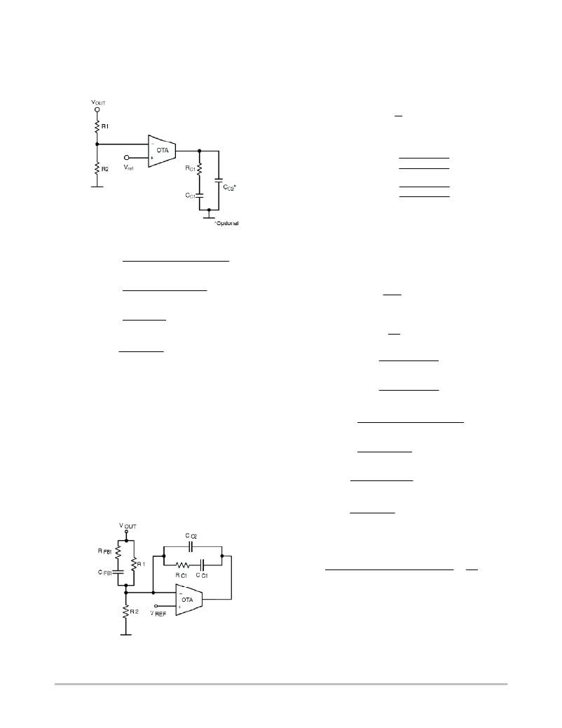
�NCP3011,� NCV3011�
�Compensation� Type� II�
�This� compensation� is� suitable� for� electrolytic� capacitors.�
�Components� of� the� Type� II� compensation� (Figure� 45)�
�network� can� be� specified� by� the� following� equations:�
�f� Z1� +� 0.75� @� f� P0�
�f� Z2� +� f� P0�
�f� P2� +� f� Z0�
�(eq.� 47)�
�(eq.� 48)�
�(eq.� 49)�
�f� P3� +�
�f� S�
�2�
�(eq.� 50)�
�Method� II� is� better� suited� for� ceramic� capacitors� that�
�typically� have� the� lowest� ESR� available:�
�f� Z2� +� f� 0� @�
�f� P2� +� f� 0� @�
�1� *� sin� q� max�
�1� )� sin� q� max�
�1� )� sin� q� max�
�1� *� sin� q� max�
�(eq.� 51)�
�(eq.� 52)�
�f� Z1� +� 0.5� @� f� Z2�
�(eq.� 53)�
�Figure� 45.� Type� II� Compensation�
�f� P3� +� 0.5� @� f� S�
�(eq.� 54)�
�R� C1� +�
�C� C1� +�
�2� @� p� @� f� 0� @� L� @� V� RAMP� @� V� OUT�
�ESR� @� V� IN� @� V� ref� @� gm�
�1�
�0.75� @� 2� @� p� @� f� P0� @� R� C1�
�(eq.� 43)�
�(eq.� 44)�
�q� max� is� the� desired� maximum� phase� margin� at� the� zero�
�crossover� frequency,� ?� 0� .� It� should� be� 45� °� ?� 75� °� .� Convert�
�degrees� to� radians� by� the� formula:�
�2� @� p�
�q� max� +� q� max� degress� @� 360� :� Units� +� radians� (eq.� 55)�
�C� C2� +�
�1�
�R� C1� u� u�
�2�
�gm�
�C� C1� +�
�1�
�C� C2� +�
�1�
�(eq.� 45)�
�p� @� R� C1� @� f� S�
�V� OUT� *� V� ref�
�R1� +� @� R2� (eq.� 46)�
�V� ref�
�V� RAMP� is� the� peak� ?� to� ?� peak� voltage� of� the� oscillator� ramp�
�and� gm� is� the� transconductance� error� amplifier� gain.�
�Capacitor� C� C2� is� optional.�
�The� remaining� calculations� are� the� same� for� both� methods.�
�(eq.� 56)�
�(eq.� 57)�
�2� @� p� @� f� Z1� @� R� C1�
�(eq.� 58)�
�2� @� p� @� f� P3� @� R� C1�
�Compensation� Type� III�
�Tantalum� and� ceramics� capacitors� have� lower� ESR� than�
�electrolytic,� so� the� zero� of� the� output� LC� filter� goes� to� a�
�C� FB1� +�
�2� @� p� @� f� 0� @� L� @� V� RAMP� @� C� OUT�
�V� IN� @� R� C1�
�(eq.� 59)�
�R� FB1� +�
�R1� +�
�higher� frequency� above� the� zero� crossover� frequency.� This�
�requires� a� Type� III� compensation� network� as� shown� in�
�Figure� 46.�
�There� are� two� methods� to� select� the� zeros� and� poles� of� this�
�compensation� network.� Method� I� is� ideal� for� tantalum�
�1�
�2� p� @� C� FB1� @� f� P2�
�1�
�2� @� p� @� C� FB1� @� f� Z2�
�*� R� FB1�
�(eq.� 60)�
�(eq.� 61)�
�V�
�output� capacitors,� which� have� a� higher� ESR� than� ceramic:�
�R2� +�
�ref�
�V� OUT� *� V� ref�
�@� R1�
�(eq.� 62)�
�If� the� equation� in� Equation� 63� is� not� true,� then� a� higher� value�
�of� R� C1� must� be� selected.�
�R1� @� R2� @� R� FB1�
�R1� @� R� FB1� )� R2� @� R� FB1� )� R1� @� R2�
�u�
�1�
�gm�
�(eq.� 63)�
�Figure� 46.� Type� III� Compensation�
�http://onsemi.com�
�26�
�相关PDF资料 |
PDF描述 |
|---|---|
| RPP50-483.3S | CONV DC/DC 50W 36-75VIN 3.3VOUT |
| RPP40-2424DW | CONV DC/DC 40W 9-36V +/-24VOUT |
| RPP40-2415DW-F | CONV DC/DC 40W 9-36V +/-15VOUT |
| RPP40-2415DW-1F | CONV DC/DC 40W 9-36V +/-15VOUT |
| RPP40-2415DW-1 | CONV DC/DC 40W 9-36V +/-15VOUT |
相关代理商/技术参数 |
参数描述 |
|---|---|
| NCP3011GEVB | 功能描述:电源管理IC开发工具 NCP3011 EVALUATION BOARD RoHS:否 制造商:Maxim Integrated 产品:Evaluation Kits 类型:Battery Management 工具用于评估:MAX17710GB 输入电压: 输出电压:1.8 V |
| NCP3012 | 制造商:ONSEMI 制造商全称:ON Semiconductor 功能描述:Synchronous PWM Controller |
| NCP3012DTBR2G | 功能描述:电压模式 PWM 控制器 Single Output Buck 0.8V to 40V 70uA RoHS:否 制造商:Texas Instruments 输出端数量:1 拓扑结构:Buck 输出电压:34 V 输出电流: 开关频率: 工作电源电压:4.5 V to 5.5 V 电源电流:600 uA 最大工作温度:+ 125 C 最小工作温度:- 40 C 封装 / 箱体:WSON-8 封装:Reel |
| NCP301HSN09T1 | 功能描述:电压监测器/监控器 0.9V Detector RoHS:否 制造商:Texas Instruments 监测电压数:2 监测电压:Adjustable 输出类型:Open Drain 欠电压阈值: 过电压阈值: 准确性:1 % 工作电源电压:1.5 V to 6.5 V 工作电源电流:1.8 uA 最大工作温度:+ 125 C 封装 / 箱体:SON-6 安装风格:SMD/SMT |
| NCP301HSN09T1G | 功能描述:电压监测器/监控器 0.9V Detector w/Reset High RoHS:否 制造商:Texas Instruments 监测电压数:2 监测电压:Adjustable 输出类型:Open Drain 欠电压阈值: 过电压阈值: 准确性:1 % 工作电源电压:1.5 V to 6.5 V 工作电源电流:1.8 uA 最大工作温度:+ 125 C 封装 / 箱体:SON-6 安装风格:SMD/SMT |
发布紧急采购,3分钟左右您将得到回复。