- 您现在的位置:买卖IC网 > Datasheet目录996 > NCP3065BBGEVB (ON Semiconductor)BOARD EVAL NCP3065 MR16 BOOST Datasheet资料下载
参数资料
| 型号: | NCP3065BBGEVB |
| 厂商: | ON Semiconductor |
| 文件页数: | 8/18页 |
| 文件大小: | 0K |
| 描述: | BOARD EVAL NCP3065 MR16 BOOST |
| 设计资源: | NCP3065BBGEVB Schematic NCP3065BBGEVB Gerber Files NCP3065BBGEVB Bill of Materials |
| 标准包装: | 1 |
| 电流 - 输出 / 通道: | 350mA |
| 输出及类型: | 1,非隔离 |
| 输出电压: | 8 ~ 12 V |
| 输入电压: | 6 ~ 16 V 或 12VAC |
| 已供物品: | 板 |
| 已用 IC / 零件: | NCP3065 |
| 其它名称: | NCP3065BBGEVB-ND NCP3065BBGEVBOS |
�� �
�
�NCP3065,� NCV3065�
�Peak� Current� Sense� Comparator�
�Under� normal� conditions,� the� output� switch� conduction� is�
�initiated� by� the� Voltage� Feedback� comparator� and�
�terminated� by� the� oscillator.� Abnormal� operating� conditions�
�occur� when� the� converter� output� is� overloaded� or� when�
�feedback� voltage� sensing� is� lost.� Under� these� conditions,� the�
�I� pk� Current� Sense� comparator� will� protect� the� Darlington�
�output� Switch.� The� switch� current� is� converted� to� a� voltage�
�by� inserting� a� fractional� ohm� resistor,� R� SC� ,� in� series� with�
�V� CC� and� the� Darlington� output� switch.� The� voltage� drop�
�across� R� SC� is� monitored� by� the� Current� Sense� comparator.�
�If� the� voltage� drop� exceeds� 200� mV� (nom)� with� respect� to�
�LED� Dimming�
�The� COMP� pin� of� the� NCP3065� is� used� to� provide�
�dimming� capability.� In� digital� input� mode� the� PWM� input�
�signal� inhibits� switching� of� the� regulator� and� reduces� the�
�average� current� through� the� LEDs.� In� analog� input� mode� a�
�PWM� input� signal� is� RC� filtered� and� the� resulting� voltage� is�
�summed� with� the� feedback� voltage� thus� reduces� the� average�
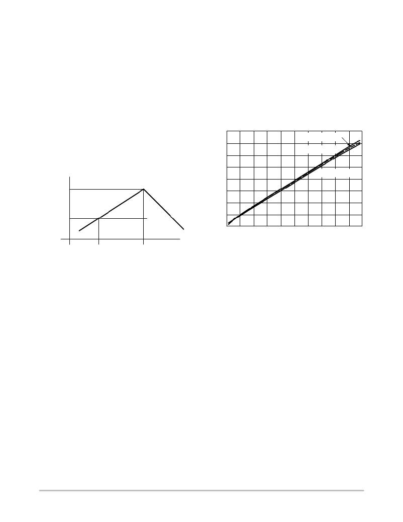
�current� through� the� LEDs.� Figure� 15� illustrated� the� linearity�
�of� the� digital� dimming� function� with� a� 200� Hz� digital� PWM.�
�For� further� information� on� dimming� control� refer� to�
�application� note� AND8298.�
�V� CC� ,� the� comparator� will� set� the� latch� and� terminate� the�
�output� switch� conduction� on� a� cycle� ?� by� ?� cycle� basis.� This�
�Comparator/Latch� configuration� ensures� that� the� Output�
�Switch� has� only� a� single� on� ?� time� during� a� given� oscillator�
�800�
�700�
�600�
�24 V� in� , V� f� = 7.2 V�
�24 V� in� , V� f� = 3.6 V�
�cycle.�
�Real�
�V� turn� ?� off� on�
�R� s� Resistor�
�di/dt� slope�
�I1�
�I� through� the�
�Darlington�
�500�
�400�
�300�
�200�
�12 V� in� , V� f� = 3.6 V�
�V� ipk(sense)�
�Io�
�t_delay�
�Switch�
�100�
�0�
�0�
�10�
�20�
�30�
�40�
�50�
�60�
�70�
�80�
�90� 100�
�DUTY� CYCLE� (%)�
�The� V� IPK(Sense)� Current� Limit� Sense� Voltage� threshold� is�
�specified� at� static� conditions.� In� dynamic� operation� the�
�sensed� current� turn� ?� off� value� depends� on� comparator�
�response� time� and� di/dt� current� slope.�
�Real� V� turn� ?� off� on� R� sc� resistor�
�Vturn_off� +� Vipk(sense)� )� Rsc� @� (t_delay� @� di� dt)�
�Typical� I� pk� comparator� response� time� t_delay� is� 350� ns.�
�The� di/dt� current� slope� is� dependent� on� the� voltage�
�difference� across� the� inductor� and� the� value� of� the� inductor.�
�Increasing� the� value� of� the� inductor� will� reduce� the� di/dt�
�slope.�
�It� is� recommended� to� verify� the� actual� peak� current� in� the�
�application� at� worst� conditions� to� be� sure� that� the� max� peak�
�current� will� never� get� over� the� 1.5� A� Darlington� Switch�
�Current� max� rating.�
�Thermal� Shutdown�
�Internal� thermal� shutdown� circuitry� is� provided� to� protect�
�the� IC� in� the� event� that� the� maximum� junction� temperature�
�is� exceeded.� When� activated,� typically� at� 165� °� C,� the�
�Darlington� Output� Switch� is� disabled.� The� temperature�
�sensing� circuit� is� designed� with� some� hysteresis.� The�
�Darlington� Switch� is� enabled� again� when� the� chip�
�temperature� decreases� under� the� low� threshold.� This� feature�
�is� provided� to� prevent� catastrophic� failures� from� accidental�
�device� overheating.� It� is� not� intended� to� be� used� as� a�
�replacement� for� proper� heatsinking.�
�Figure� 15.�
�No� Output� Capacitor� Operation�
�A� constant� current� buck� regulator� such� as� the� NCP3065�
�focuses� on� the� control� of� the� current� through� the� load,� not� the�
�voltage� across� it.� The� switching� frequency� of� the� NCP3065�
�is� in� the� range� of� 100� ?� 250� kHz� which� is� much� higher� than�
�the� human� eye� can� detect.� This� allows� us� to� relax� the� ripple�
�current� specification� to� allow� higher� peak� to� peak� values.�
�This� is� achieved� by� configuring� the� NCP3065� in� a�
�continuous� conduction� buck� configuration� with� low� peak� to�
�peak� ripple� thus� eliminating� the� need� for� an� output� filter�
�capacitor.� The� important� design� parameter� is� to� keep� the�
�peak� current� below� the� maximum� current� rating� of� the� LED.�
�Using� 15%� peak� to� peak� ripple� results� in� a� good� compromise�
�between� achieving� max� average� output� current� without�
�exceeding� the� maximum� limit.� This� saves� space� and� reduces�
�part� count� for� applications� that� require� a� compact� footprint.�
�(Example:� See� Figure� 17)� See� application� note� AND8298�
�for� more� information.�
�Output� Switch�
�The� output� switch� is� designed� in� a� Darlington�
�configuration.� This� allows� the� application� designer� to�
�operate� at� all� conditions� at� high� switching� speed� and� low�
�voltage� drop.� The� Darlington� Output� Switch� is� designed� to�
�switch� a� maximum� of� 40� V� collector� to� emitter� voltage� and�
�current� up� to� 1.5� A.�
�http://onsemi.com�
�8�
�相关PDF资料 |
PDF描述 |
|---|---|
| NCP3066SCBCKGEVB | EVAL BOARD FOR NCP3066SCBCKG |
| NCP5005GEVB | EVAL BOARD FOR NCP5005G |
| NCP5006EVB | EVAL BOARD FOR NCP5006 |
| NCP5030MTTXGEVB | EVAL BOARD FOR NCP5030MTTXG |
| NCP5602EVB | EVAL BOARD FOR NCP5602 |
相关代理商/技术参数 |
参数描述 |
|---|---|
| NCP3065D1SLDGEVB | 功能描述:电源管理IC开发工具 SEPIC LED DRV MR16BULB RoHS:否 制造商:Maxim Integrated 产品:Evaluation Kits 类型:Battery Management 工具用于评估:MAX17710GB 输入电压: 输出电压:1.8 V |
| NCP3065D2SLDGEVB | 功能描述:电源管理IC开发工具 SEPIC LED DRV 350MA RoHS:否 制造商:Maxim Integrated 产品:Evaluation Kits 类型:Battery Management 工具用于评估:MAX17710GB 输入电压: 输出电压:1.8 V |
| NCP3065D3SLDGEVB | 功能描述:电源管理IC开发工具 SEPIC LED DRV 700MA RoHS:否 制造商:Maxim Integrated 产品:Evaluation Kits 类型:Battery Management 工具用于评估:MAX17710GB 输入电压: 输出电压:1.8 V |
| NCP3065DR2G | 功能描述:直流/直流开关调节器 1.5A SW REG FOR LED APPL RoHS:否 制造商:International Rectifier 最大输入电压:21 V 开关频率:1.5 MHz 输出电压:0.5 V to 0.86 V 输出电流:4 A 输出端数量: 最大工作温度: 安装风格:SMD/SMT 封装 / 箱体:PQFN 4 x 5 |
| NCP3065DR2G | 制造商:ON Semiconductor 功能描述:DC/DC Converter IC |
发布紧急采购,3分钟左右您将得到回复。