- 您现在的位置:买卖IC网 > Datasheet目录996 > NCP3065BBGEVB (ON Semiconductor)BOARD EVAL NCP3065 MR16 BOOST Datasheet资料下载
参数资料
| 型号: | NCP3065BBGEVB |
| 厂商: | ON Semiconductor |
| 文件页数: | 9/18页 |
| 文件大小: | 0K |
| 描述: | BOARD EVAL NCP3065 MR16 BOOST |
| 设计资源: | NCP3065BBGEVB Schematic NCP3065BBGEVB Gerber Files NCP3065BBGEVB Bill of Materials |
| 标准包装: | 1 |
| 电流 - 输出 / 通道: | 350mA |
| 输出及类型: | 1,非隔离 |
| 输出电压: | 8 ~ 12 V |
| 输入电压: | 6 ~ 16 V 或 12VAC |
| 已供物品: | 板 |
| 已用 IC / 零件: | NCP3065 |
| 其它名称: | NCP3065BBGEVB-ND NCP3065BBGEVBOS |
�� �
�
�NCP3065,� NCV3065�
�APPLICATIONS�
�Figures� 16� through� 24� show� the� simplicity� and� flexibility�
�of� the� NCP3065.� Two� main� converter� topologies� are�
�demonstrated� with� actual� test� data� shown� below� each� of� the�
�circuit� diagrams.�
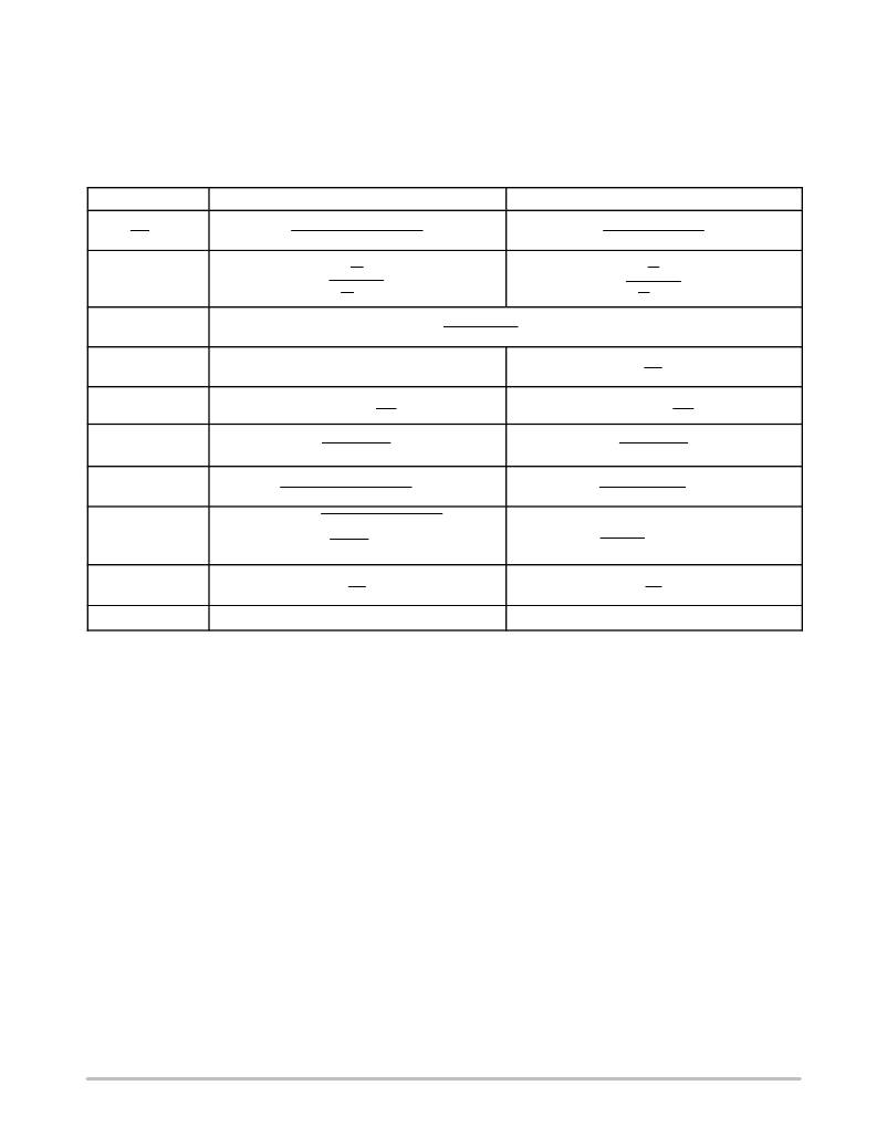
�Figure� 16� gives� the� relevant� design� equations� for� the� key�
�parameters.� Additionally,� a� complete� application� design� aid�
�for� the� NCP3065� can� be� found� at� www.onsemi.com.�
�(See� Notes� 8,� 9,� 10)�
�ton�
�toff�
�t� on�
�Step� ?� Down�
�Vout� )� VF�
�Vin� *� VSWCE� *� Vout�
�ton�
�toff�
�Step� ?� Up�
�Vout� )� VF� *� Vin�
�Vin� *� VSWCE�
�ton�
�toff�
�CT� +� 381.6� @� 10�
�C� T�
�f�
�ton�
�toff�
�)� 1�
�fosc�
�*� 6�
�*� 343� @� 10� *� 12�
�f�
�ton�
�toff�
�)� 1�
�I� L(avg)�
�Iout�
�Iout�
�ton�
�toff�
�)� 1�
�I� pk� (Switch)�
�IL(avg)� )�
�D� IL�
�2�
�IL(avg)� )�
�D� IL�
�2�
�R� SC�
�0.20�
�Ipk� (Switch)�
�0.20�
�Ipk� (Switch)�
�L�
�Vin� *� VSWCE� *� Vout�
�D� IL�
�ton�
�Vin� *� VSWCE�
�D� IL�
�ton�
�V� ripple(pp)�
�D� IL�
�1�
�8� f� CO�
�2�
�)� (ESR)� 2�
�[�
�ton Iout�
�CO�
�)� D� IL� @� ESR�
�V� out�
�VTH�
�R2�
�R1�
�)� 1�
�VTH�
�R2�
�R1�
�)� 1�
�I� out�
�V� ref� R� sense�
�V� ref� R� sense�
�8.� V� SWCE� ?� Darlington� Switch� Collector� to� Emitter� Voltage� Drop,� refer� to� Figures� 7,� 8,� 9� and� 10.�
�9.� V� F� ?� Output� rectifier� forward� voltage� drop.� Typical� value� for� 1N5819� Schottky� barrier� rectifier� is� 0.4� V.�
�10.� The� calculated� t� on� /t� off� must� not� exceed� the� minimum� guaranteed� oscillator� charge� to� discharge� ratio.�
�Figure� 16.� Design� Equations�
�The� Following� Converter� Characteristics� Must� Be� Chosen:�
�V� in� ?� Nominal� operating� input� voltage.�
�V� out� ?� Desired� output� voltage.�
�I� out� ?� Desired� output� current.�
�D� I� L� ?� Desired� peak� ?� to� ?� peak� inductor� ripple� current.� For� maximum� output� current� it� is� suggested� that� D� I� L� be� chosen� to� be�
�less� than� 10%� of� the� average� inductor� current� I� L(avg)� .� This� will� help� prevent� I� pk� (Switch)� from� reaching� the� current� limit� threshold�
�set� by� R� SC� .� If� the� design� goal� is� to� use� a� minimum� inductance� value,� let� D� I� L� =� 2(I� L(avg)� ).� This� will� proportionally� reduce�
�converter� output� current� capability.�
�f� ?� Maximum� output� switch� frequency.�
�V� ripple(pp)� ?� Desired� peak� ?� to� ?� peak� output� ripple� voltage.� For� best� performance� the� ripple� voltage� should� be� kept� to� a� low�
�value� since� it� will� directly� affect� line� and� load� regulation.� Capacitor� C� O� should� be� a� low� equivalent� series� resistance� (ESR)�
�electrolytic� designed� for� switching� regulator� applications.�
�http://onsemi.com�
�9�
�相关PDF资料 |
PDF描述 |
|---|---|
| NCP3066SCBCKGEVB | EVAL BOARD FOR NCP3066SCBCKG |
| NCP5005GEVB | EVAL BOARD FOR NCP5005G |
| NCP5006EVB | EVAL BOARD FOR NCP5006 |
| NCP5030MTTXGEVB | EVAL BOARD FOR NCP5030MTTXG |
| NCP5602EVB | EVAL BOARD FOR NCP5602 |
相关代理商/技术参数 |
参数描述 |
|---|---|
| NCP3065D1SLDGEVB | 功能描述:电源管理IC开发工具 SEPIC LED DRV MR16BULB RoHS:否 制造商:Maxim Integrated 产品:Evaluation Kits 类型:Battery Management 工具用于评估:MAX17710GB 输入电压: 输出电压:1.8 V |
| NCP3065D2SLDGEVB | 功能描述:电源管理IC开发工具 SEPIC LED DRV 350MA RoHS:否 制造商:Maxim Integrated 产品:Evaluation Kits 类型:Battery Management 工具用于评估:MAX17710GB 输入电压: 输出电压:1.8 V |
| NCP3065D3SLDGEVB | 功能描述:电源管理IC开发工具 SEPIC LED DRV 700MA RoHS:否 制造商:Maxim Integrated 产品:Evaluation Kits 类型:Battery Management 工具用于评估:MAX17710GB 输入电压: 输出电压:1.8 V |
| NCP3065DR2G | 功能描述:直流/直流开关调节器 1.5A SW REG FOR LED APPL RoHS:否 制造商:International Rectifier 最大输入电压:21 V 开关频率:1.5 MHz 输出电压:0.5 V to 0.86 V 输出电流:4 A 输出端数量: 最大工作温度: 安装风格:SMD/SMT 封装 / 箱体:PQFN 4 x 5 |
| NCP3065DR2G | 制造商:ON Semiconductor 功能描述:DC/DC Converter IC |
发布紧急采购,3分钟左右您将得到回复。