- 您现在的位置:买卖IC网 > PDF目录17260 > NCP5181DR2G (ON Semiconductor)IC MOSFET DRVR HIGH VOLT 8-SOIC PDF资料下载
参数资料
| 型号: | NCP5181DR2G |
| 厂商: | ON Semiconductor |
| 文件页数: | 4/12页 |
| 文件大小: | 0K |
| 描述: | IC MOSFET DRVR HIGH VOLT 8-SOIC |
| 标准包装: | 1 |
| 配置: | 半桥 |
| 输入类型: | 非反相 |
| 延迟时间: | 100ns |
| 电流 - 峰: | 1.4A |
| 配置数: | 1 |
| 输出数: | 2 |
| 高端电压 - 最大(自引导启动): | 600V |
| 电源电压: | 10 V ~ 20 V |
| 工作温度: | -40°C ~ 125°C |
| 安装类型: | 表面贴装 |
| 封装/外壳: | 8-SOIC(0.154",3.90mm 宽) |
| 供应商设备封装: | 8-SOICN |
| 包装: | 标准包装 |
| 其它名称: | NCP5181DR2GOSDKR |
�� �
�
�NCP5181�
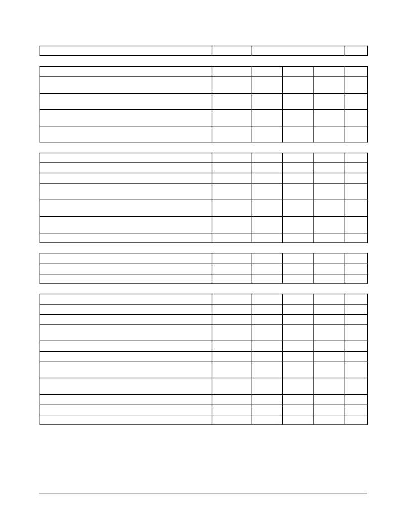
�ELECTRICAL� CHARACTERISTICS� (V� CC� =� V� boot� =� 15� V,� V� gnd� =� V� bridge� ,� ?� 40� °� C� <� T� A� <� 125� °� C,� Outputs� loaded� with� 1� nF)�
�Rating�
�Symbol�
�T� A� ?� 40� °� C� to� 125� °� C�
�Units�
�OUTPUT� SECTION�
�Min�
�Typ�
�Max�
�Output� High� Short� Circuit� pulsed� Current�
�V� DRV� =� 0� V,� PW� ≤� 10� m� s,� (Note� 1)�
�Output� Low� Short� Circuit� Pulsed� Current�
�V� DRV� =� V� CC� ,� PW� ≤� 10� m� s,� (Note� 1)�
�Output� Resistor� (Typical� Value� @� 25� °� C� Only)�
�Source�
�Output� Resistor� (Typical� Value� @� 25� °� C� Only)�
�Sink�
�I� DRVhigh�
�I� DRVlow�
�R� OH�
�R� OL�
�?�
�?�
�?�
�?�
�1.4�
�2.2�
�5�
�2�
�?�
�?�
�12�
�8�
�A�
�A�
�W�
�W�
�DYNAMIC� OUTPUT� SECTION�
�Rating�
�Turn� ?� on� Propagation� Delay� (V� bridge� =� 0� V)�
�Turn� ?� off� Propagation� Delay� (V� bridge� =� 0� V� or� 50� V)� (Note� 2)�
�Output� Voltage� Risetime�
�(from� 10%� to� 90%� @� V� CC� =� 15� V)� with� 1� nF� Load�
�Output� Voltage� Falling� Edge�
�(from� 90%� to� 10%� @� V� CC� =� 15� V)� with� 1� nF� Load�
�Propagation� Delay� Matching� between� the� High� Side� and� the� Low� Side�
�@� 25� °� C� (Note� 3)�
�Minimum� Input� Pulse� Width� that� Changes� the� Output�
�Symbol�
�t� ON�
�t� OFF�
�t� r�
�t� f�
�D� t�
�t� PW�
�Min�
�?�
�?�
�?�
�?�
�?�
�?�
�Typ�
�100�
�100�
�40�
�20�
�20�
�?�
�Max�
�170�
�170�
�60�
�40�
�35�
�100�
�Units�
�ns�
�ns�
�ns�
�ns�
�ns�
�ns�
�INPUT� SECTION�
�Low� Level� Input� Voltage� Threshold�
�Input� Pulldown� Resistor� (V� IN� <� 0.5� V)�
�High� Level� Input� Voltage� Threshold�
�V� IN�
�R� IN�
�V� IN�
�?�
�?�
�2.3�
�?�
�200�
�?�
�0.8�
�?�
�?�
�V�
�k� W�
�V�
�SUPPLY� SECTION�
�V� CC� UV� Startup� Voltage� Threshold�
�V� CC� UV� Shutdown� Voltage� Threshold�
�Hysteresis� on� V� CC�
�V� boot� Startup� Voltage� Threshold� Reference� to� Bridge� Pin�
�(V� boot_stup� =� V� boot� ?� V� bridge� )�
�V� boot� UV� Shutdown� Voltage� Threshold�
�Hysteresis� on� V� boot�
�Leakage� Current� on� High� Voltage� Pins� to� GND�
�(V� BOOT� =� V� BRIDGE� =� DRV_HI� =� 600� V)�
�Consumption� in� Active� Mode�
�(V� CC� =� V� boot� ,� f� sw� =� 100� kHz� and� 1� nF� Load� on� Both� Driver� Outputs)�
�Consumption� in� Inhibition� Mode� (V� CC� =� V� boot� )�
�V� CC� Current� Consumption� in� Inhibition� Mode�
�V� boot� Current� Consumption� in� Inhibition� Mode�
�V� CC_stup�
�V� CC_shtdwn�
�V� CC_hyst�
�V� boot_stup�
�V� boot_shtdwn�
�V� boot_shtdwn�
�I� HV_LEAK�
�I� CC1�
�I� CC2�
�I� CC3�
�I� CC4�
�7.9�
�7.3�
�0.3�
�7.9�
�7.3�
�0.3�
�?�
�?�
�?�
�?�
�?�
�8.9�
�8.2�
�0.7�
�8.9�
�8.2�
�0.7�
�0.5�
�4.5�
�250�
�215�
�35�
�9.8�
�9.0�
�?�
�9.8�
�9.0�
�?�
�40�
�6.5�
�400�
�?�
�?�
�V�
�V�
�V�
�V�
�V�
�V�
�m� A�
�mA�
�m� A�
�m� A�
�m� A�
�*Note:� see� also� characterization� curves�
�1.� Guaranteed� by� design.�
�2.� Turn� ?� off� propagation� delay� @� V� bridge� =� 600� V� is� guaranteed� by� design�
�3.� See� characterization� curve� for� D� t� parameters� variation� on� the� full� range� temperature.�
�4.� Timing� diagram� definition� see� Figures� 4,� 5� and� 6.�
�http://onsemi.com�
�4�
�相关PDF资料 |
PDF描述 |
|---|---|
| CB2016T1R0M | INDUCTOR POWER 1.0UH 1.1A 0806 |
| GCM10DCWI | CONN EDGECARD 20POS DIP .156 SLD |
| 100R12-457B | CABLE FLAT FLEX 12POS 1MM 18" |
| LK16083R3K-T | INDUCTOR 3.3UH 10% 0603 SMD |
| R1D12-2415-R | CONV DC/DC 1W 24VIN +/-15VOUT |
相关代理商/技术参数 |
参数描述 |
|---|---|
| NCP5181DR2G-CUT TAPE | 制造商:ON 功能描述:NCP Series 2.2 A 20 V 2 Ohm SMT High Voltage High and Low Side Driver - SOIC-8 |
| NCP5181PG | 功能描述:功率驱动器IC HV MOSFET DRIVER RoHS:否 制造商:Micrel 产品:MOSFET Gate Drivers 类型:Low Cost High or Low Side MOSFET Driver 上升时间: 下降时间: 电源电压-最大:30 V 电源电压-最小:2.75 V 电源电流: 最大功率耗散: 最大工作温度:+ 85 C 安装风格:SMD/SMT 封装 / 箱体:SOIC-8 封装:Tube |
| NCP5201 | 制造商:ONSEMI 制造商全称:ON Semiconductor 功能描述:Dual Output DDR Power Controller |
| NCP5201/D | 制造商:未知厂家 制造商全称:未知厂家 功能描述:Dual Output DDR Power Controller |
| NCP5201_06 | 制造商:ONSEMI 制造商全称:ON Semiconductor 功能描述:Dual Output DDR Power Controller |
发布紧急采购,3分钟左右您将得到回复。