- 您现在的位置:买卖IC网 > Datasheet目录346 > NCV8855BMNR2GEVB (ON Semiconductor)BOARD EVALUATION NCV8855 ASIC Datasheet资料下载
参数资料
| 型号: | NCV8855BMNR2GEVB |
| 厂商: | ON Semiconductor |
| 文件页数: | 8/24页 |
| 文件大小: | 0K |
| 描述: | BOARD EVALUATION NCV8855 ASIC |
| 设计资源: | NCV8855BMNR2GEVB Schematic NCV8855 BOM |
| 标准包装: | 1 |
| 主要目的: | DC/DC,LDO 步降 |
| 输出及类型: | 4,非隔离 |
| 电流 - 输出: | 2.5A |
| 输入电压: | 9 V ~ 18 V |
| 稳压器拓扑结构: | 降压 |
| 频率 - 开关: | 170kHz |
| 板类型: | 完全填充 |
| 已供物品: | 板 |
| 已用 IC / 零件: | NCV8855 |
| 其它名称: | NCV8855BMNR2GEVBOS |
�� �
�
�NCV8855�
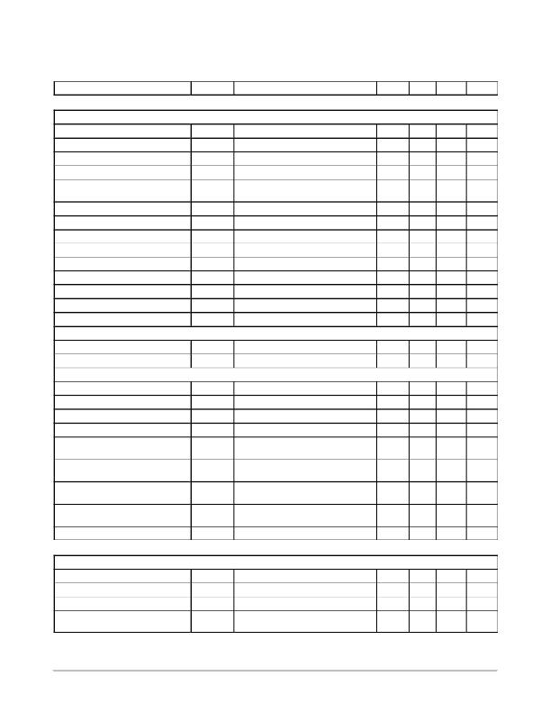
�ELECTRICAL� CHARACTERISTICS� (V� IN_SW� =� V� IN� =� V� ISNS1+� =� V� ISNS1� ?� =� V� ISNS2+� =� V� ISNS2� ?� =� 13.2� V,� SYS_EN� =� LDO_EN� =�
�HS_EN� =� 5� V,� VOUT3� =� 3.3� V,� VOUT4� =� 8.5� V,� IOUT[1:4]� =� 0� A)� Min/Max� values� are� valid� for� the� temperature� range� ?� 40� °� C� v� T� J� v�
�150� °� C� unless� noted� otherwise.� Min/Max� values� are� guaranteed� by� test,� design� or� statistical� correlation.�
�Parameter�
�Symbol�
�Conditions�
�Min�
�Typ�
�Max�
�Unit�
�SWITCH� ?� MODE� POWER� SUPPLY� CONTROLLER� (SMPS1,� VOUT1)� SPECIFICATIONS�
�Error� Amplifier�
�Dc� gain�
�Gain� ?� bandwidth� product�
�SW_FB1� input� bias� current�
�Input� offset� voltage�
�(Note� 1)�
�(Note� 1)�
�SW_FB1� =� 0.8� V�
�(Note� 1)�
�70�
�8�
�85�
�10�
�100�
�800�
�dB�
�MHz�
�nA�
�m� V�
�Slew� rate�
�COMP1� source� current�
�COMP1� sink� current�
�C� COMP1� =� 50� pF,� $� 1� mA� dc� load� Slew� rate�
�within� ramp� voltage� levels� (Note� 1)�
�V� COMP1� =� 2.2� V�
�V� COMP1� =� 3.2� V�
�V� COMP1� =� 2.2� V�
�V� COMP1� =� 1.1� V�
�6�
�1.5�
�1.6�
�1.1�
�0.7�
�8�
�8�
�8�
�8�
�8�
�V/� m� s�
�mA�
�mA�
�mA�
�mA�
�Minimum� COMP1� voltage�
�Maximum� COMP1� voltage�
�I� COMP1� =� 500� m� A�
�I� COMP1� =� 2� mA�
�3.3�
�1.05�
�V�
�V�
�Ramp� maximum� voltage�
�Ramp� minimum� voltage�
�2.8�
�1.1�
�3.0�
�1.2�
�3.2�
�1.3�
�V�
�V�
�Ramp� voltage� amplitude�
�V� RAMP1�
�1.6�
�1.8�
�2.0�
�V�
�Duty� Cycle� Limitations�
�Minimum� off� time�
�Minimum� pulse� width�
�t� MINOFF1�
�t� MINON1�
�GH1� falling� to� GL1� rising�
�GH1� rising� to� GH1� falling�
�80�
�120�
�140�
�250�
�200�
�300�
�ns�
�ns�
�Gate� Driver�
�GH1� source� current�
�GH1� sink� current�
�GL1� source� current�
�GL1� sink� current�
�V� GH1� –� V� SN1� =� 4� V,� T� J� =� 25� °� C�
�V� GH1� –� V� SN1� =� 2� V,� T� J� =� 25� °� C�
�V� GL1� –� PGND� =� 4� V,� T� J� =� 25� °� C�
�V� GL1� –� PGND� =� 1� V,� T� J� =� 25� °� C�
�1.5�
�1.5�
�1.5�
�1.5�
�A�
�A�
�A�
�A�
�SN1� falling� to� GL1� rising,� non� ?� overlap�
�time�
�GL1� falling� to� GH1� rising,� non� ?� overlap�
�time�
�SN1� falling� non� ?� overlap� threshold�
�voltage�
�GL1� falling� non� ?� overlap� threshold�
�voltage�
�SN1� falling� override� timer�
�t� NOLT�
�1.0�
�50�
�30�
�30�
�1.8�
�2�
�100�
�70�
�70�
�3.0�
�150�
�ns�
�ns�
�V�
�V�
�ns�
�SWITCH� ?� MODE� POWER� SUPPLY� REGULATOR� (SMPS2,� VOUT2)� SPECIFICATIONS�
�Over� Current� Protection�
�Internal� current� limit�
�Current� limit� blanking� time�
�2.5�
�100�
�3.05�
�4.2�
�200�
�A�
�ns�
�Short� circuit� threshold� voltage�
�Short� circuit� protection� startup� delay�
�SCTH2�
�V� SW_FB2� %� of� V� REF�
�From� SYS_EN� rising� edge,� %� of� t� SS2,�
�SW_FB2� =� 0.5� V�
�75�
�100�
�85�
�125�
�95�
�150�
�%�
�%�
�1.� Guaranteed� by� design,� not� fully� tested� in� production.�
�2.� Indirectly� guaranteed� by� test� coverage� of� other� parameters.�
�http://onsemi.com�
�8�
�相关PDF资料 |
PDF描述 |
|---|---|
| NCV8871BSTGEVB | BOARD EVAL NCV8871BST BOOST CTLR |
| NHC-14150 | VALULINE 8" X 8.5" X 1.75" |
| NHC-14151 | VALULINE 8" X 17" X 1.75" |
| NHC-14152 | VALULINE 13" X 17" X 1.75" |
| NHC-14153 | VALULINE 8" X 8.5" X 3.5" |
相关代理商/技术参数 |
参数描述 |
|---|---|
| NCV8870 | 制造商:ONSEMI 制造商全称:ON Semiconductor 功能描述:Automotive Grade Non-Synchronous Boost Controller |
| NCV887000 | 制造商:ONSEMI 制造商全称:ON Semiconductor 功能描述:Automotive Grade Non-Synchronous Boost Controller |
| NCV887000D1R2G | 功能描述:低压差稳压器 - LDO Auto Grade Non-Sync Boost Controller RoHS:否 制造商:Texas Instruments 最大输入电压:36 V 输出电压:1.4 V to 20.5 V 回动电压(最大值):307 mV 输出电流:1 A 负载调节:0.3 % 输出端数量: 输出类型:Fixed 最大工作温度:+ 125 C 安装风格:SMD/SMT 封装 / 箱体:VQFN-20 |
| NCV887001 | 制造商:ONSEMI 制造商全称:ON Semiconductor 功能描述:Automotive Grade Non-Synchronous Boost Controller |
| NCV887001D1R2G | 功能描述:低压差稳压器 - LDO Auto Grade Non-Sync Boost Controller RoHS:否 制造商:Texas Instruments 最大输入电压:36 V 输出电压:1.4 V to 20.5 V 回动电压(最大值):307 mV 输出电流:1 A 负载调节:0.3 % 输出端数量: 输出类型:Fixed 最大工作温度:+ 125 C 安装风格:SMD/SMT 封装 / 箱体:VQFN-20 |
发布紧急采购,3分钟左右您将得到回复。