- 您现在的位置:买卖IC网 > Datasheet目录45 > NCV8881PWR2G (ON Semiconductor)IC REG TRPL BUCK/LINEAR 16SOIC Datasheet资料下载
参数资料
| 型号: | NCV8881PWR2G |
| 厂商: | ON Semiconductor |
| 文件页数: | 32/33页 |
| 文件大小: | 321K |
| 描述: | IC REG TRPL BUCK/LINEAR 16SOIC |
| 标准包装: | 1 |
| 拓扑: | 降压(降压)(1),线性(LDO)(2) |
| 功能: | 车载 |
| 输出数: | 3 |
| 频率 - 开关: | 170kHz |
| 电压/电流 - 输出 1: | 3.3 V ~ 8 V,1.5A |
| 电压/电流 - 输出 2: | 5V,100mA |
| 电压/电流 - 输出 3: | 8.5V,40mA |
| 带 LED 驱动器: | 无 |
| 带监控器: | 无 |
| 带序列发生器: | 无 |
| 电源电压: | 5 V ~ 19 V |
| 工作温度: | -40°C ~ 150°C |
| 安装类型: | 表面贴装 |
| 封装/外壳: | 16-SOIC(0.295",7.50mm 宽)裸露焊盘 |
| 供应商设备封装: | 16-SOIC W |
| 包装: | 标准包装 |
| 其它名称: | NCV8881PWR2GOSDKR |
第1页第2页第3页第4页第5页第6页第7页第8页第9页第10页第11页第12页第13页第14页第15页第16页第17页第18页第19页第20页第21页第22页第23页第24页第25页第26页第27页第28页第29页第30页第31页当前第32页第33页
NCV8881
http://onsemi.com
32
Error Amplifier
Closed Loop Gain
Compensation Network
Modulator Gain
w
dB
OUT
ESR
C
ESR
=
1
w
OUT
OUT
LC
C
L
=
1
w
2
2
1
1
C
R
Z
=
w
( )
3
3
1
2
1
C
R
R
Z
+
=
w
?/DIV>
?/DIV>
?/DIV>
?/DIV>
?/DIV>
?/DIV>
?/DIV>
?/DIV>
+
=
2
1
2
1
2
1
1
C
C
C
C
R
P
w
3
3
2
1
C
R
P
=
w
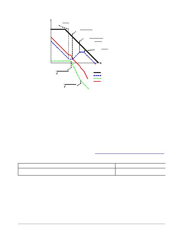
Figure 59.
To reiterate, there are 3 primary goals to compensating.
Goal 1 is to have a high a unity gain bandwidth (UGB) that
is greater than 1/10 the switching frequency F
SW
, but less
than 1/2 the switching frequency. UGB is also known as the
crossover frequency. This is the point where the loop gain =
0 dB or a gain of 1. In the plot above, the UGB is the point
where the red line crosses the TBD axis. Goal 2 is to have the
loop gain cross 0 dB with a 20 dB/decade slope also known
as a 1 slope. Goal 3 is to achieve over 45?of phase margin
when the gain crosses 0 dB. These are just goals. Sometimes
the crossover frequency is reduced below 1/10 F
SW
in order
to meet goal 3.
Conversely, some designs will push the crossover
frequency as high as it can (as long as it is below 1/2 F
SW
)
with a reduced phase margin of 30?in order to get a faster
transient response. The only two absolutes are that the
crossover frequency cannot exceed 1/2 F
SW
and the phase
margin has to be greater than 0?at crossover. However, a
SMPS operating towards these absolutes will experience
severe ringing before it dampens out.
To achieve the above goals, the following guidelines
should be adopted.
Place w
Z1
at half the resonance of w
LC
Place w
Z2
at or around w
LC
Place w
P1
at w
ESR
Place w
P2
at half the switching frequency
Performing these calculations will take some amount of
iteration and bench testing is needed to verify results.
ON Semiconductor has developed a tool to speed up the
design process tremendously with great ease and accuracy.
This tool can be downloaded by following the link below:
http://www.onsemi.com/pub/Collateral/COMPCALC.ZIP
ORDERING INFORMATION
Device
Package
Shipping
NCV8881PWR2G
SOIC16W EP
(PbFree)
1000 / Tape & Reel
For information on tape and reel specifications, including part orientation and tape sizes, please refer to our Tape and Reel Packaging
Specifications Brochure, BRD8011/D.
相关PDF资料 |
PDF描述 |
|---|---|
| NE1617ADS,112 | IC TEMP MONITOR 16SSOP |
| NE1619DS,118 | IC TEMP MONITOR 16SSOP |
| NIS5112D1R2G | IC ELECTRONIC FUSE HOTSWAP 8SOIC |
| NIS5132MN2TXG | IC ELECTRONIC FUSE 12V 10DFN |
| NIS5132MN3TXG | IC ELECTRONIC FUSE 12V 10-DFN |
相关代理商/技术参数 |
参数描述 |
|---|---|
| NCV890100 | 制造商:ONSEMI 制造商全称:ON Semiconductor 功能描述:1.2A, 2MHz Automotive Buck Switching Regulator |
| NCV890100MWTXG | 功能描述:IC REG BUCK ADJ 1.2A 8-DFN RoHS:是 类别:集成电路 (IC) >> PMIC - 稳压器 - DC DC 开关稳压器 系列:- 标准包装:50 系列:- 类型:升压(升压) 输出类型:可调式 输出数:1 输出电压:5 V ~ 25 V 输入电压:2.3 V ~ 5.5 V PWM 型:电流模式 频率 - 开关:600kHz,1.2MHz 电流 - 输出:1A 同步整流器:无 工作温度:-40°C ~ 85°C 安装类型:表面贴装 封装/外壳:8-TSSOP,8-MSOP(0.118",3.00mm 宽) 包装:管件 供应商设备封装:8-MSOP |
| NCV890100PDR2G | 功能描述:直流/直流开关调节器 Auto Buck Switching Regulator 1.2A 2 MHz RoHS:否 制造商:International Rectifier 最大输入电压:21 V 开关频率:1.5 MHz 输出电压:0.5 V to 0.86 V 输出电流:4 A 输出端数量: 最大工作温度: 安装风格:SMD/SMT 封装 / 箱体:PQFN 4 x 5 |
| NCV890101 | 制造商:ONSEMI 制造商全称:ON Semiconductor 功能描述:1.2A, 2MHz Automotive Buck Switching Regulator |
| NCV890101MWTXG | 功能描述:IC REG BUCK ADJ 1.2A 10DFN RoHS:是 类别:集成电路 (IC) >> PMIC - 稳压器 - DC DC 开关稳压器 系列:- 产品培训模块:Lead (SnPb) Finish for COTS Obsolescence Mitigation Program 标准包装:2,500 系列:- 类型:降压(降压) 输出类型:两者兼有 输出数:1 输出电压:5V,1 V ~ 10 V 输入电压:3.5 V ~ 28 V PWM 型:电流模式 频率 - 开关:220kHz ~ 1MHz 电流 - 输出:600mA 同步整流器:无 工作温度:-40°C ~ 125°C 安装类型:表面贴装 封装/外壳:16-SSOP(0.154",3.90mm 宽) 包装:带卷 (TR) 供应商设备封装:16-QSOP |
发布紧急采购,3分钟左右您将得到回复。