- 您现在的位置:买卖IC网 > PDF目录19203 > NDB6020P (Fairchild Semiconductor)MOSFET P-CH 20V 24A D2PAK PDF资料下载
参数资料
| 型号: | NDB6020P |
| 厂商: | Fairchild Semiconductor |
| 文件页数: | 1/6页 |
| 文件大小: | 0K |
| 描述: | MOSFET P-CH 20V 24A D2PAK |
| 产品培训模块: | High Voltage Switches for Power Processing |
| 产品目录绘图: | D2PAK, TO-263AB Pkg |
| 标准包装: | 1 |
| FET 型: | MOSFET P 通道,金属氧化物 |
| FET 特点: | 逻辑电平门 |
| 漏极至源极电压(Vdss): | 20V |
| 电流 - 连续漏极(Id) @ 25° C: | 24A |
| 开态Rds(最大)@ Id, Vgs @ 25° C: | 50 毫欧 @ 12A,4.5V |
| Id 时的 Vgs(th)(最大): | 1V @ 250µA |
| 闸电荷(Qg) @ Vgs: | 35nC @ 5V |
| 输入电容 (Ciss) @ Vds: | 1590pF @ 10V |
| 功率 - 最大: | 60W |
| 安装类型: | 表面贴装 |
| 封装/外壳: | TO-263-3,D²Pak(2 引线+接片),TO-263AB |
| 供应商设备封装: | D²PAK |
| 包装: | 标准包装 |
| 产品目录页面: | 1607 (CN2011-ZH PDF) |
| 其它名称: | NDB6020PDKR |
�� �
�
�September� 1997�
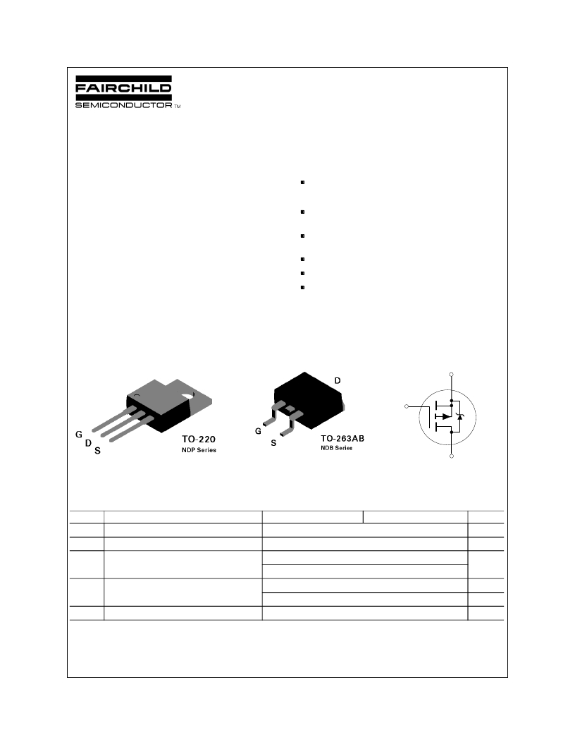
�NDP6020P� /� NDB6020P�
�P-Channel� Logic� Level� Enhancement� Mode� Field� Effect� Transistor�
�General� Description�
�These� logic� level� P-Channel� enhancement� mode� power� field�
�effect� transistors� are� produced� using� Fairchild's� proprietary,�
�high� cell� density,� DMOS� technology.� This� very� high� density�
�process� has� been� especially� tailored� to� minimize� on-state�
�resistance,� provide� superior� switching� performance,� and�
�withstand� high� energy� pulses� in� the� avalanche� and�
�commutation� modes.� These� devices� are� particularly� suited� for�
�low� voltage� applications� such� as� automotive,� DC/DC�
�converters,� PWM� motor� controls,� and� other� battery� powered�
�circuits� where� fast� switching,� low� in-line� power� loss,� and�
�resistance� to� transients� are� needed.�
�Features�
�-24� A,� -20� V.� R� DS(ON)� =� 0.05� ?� @� V� GS� =� -4.5� V.�
�R� DS(ON)� =� 0.07� ?� @� V� GS� =� -2.7� V.�
�R� DS(ON)� =� 0.075� ?� @� V� GS� =� -2.5� V.�
�Critical� DC� electrical� parameters� specified� at� elevated�
�temperature.�
�Rugged� internal� source-drain� diode� can� eliminate� the� need�
�for� an� external� Zener� diode� transient� suppressor.�
�175°C� maximum� junction� temperature� rating.�
�High� density� cell� design� for� extremely� low� R� DS(ON)� .�
�TO-220� and� TO-263� (D� 2� PAK)� package� for� both� through�
�hole� and� surface� mount� applications.�
�________________________________________________________________________________�
�S�
�G�
�D�
�Absolute� Maximum� Ratings�
�T� C� =� 25°C� unless� otherwise� noted�
�Symbol�
�V� DSS�
�V� GSS�
�Parameter�
�Drain-Source� Voltage�
�Gate-Source� Voltage� -� Continuous�
�NDP6020P�
�-20�
�±8�
�NDB6020P�
�Units�
�V�
�V�
�I� D�
�Drain� Current�
�-� Continuous�
�-24�
�A�
�-� Pulsed�
�-70�
�P� D�
�T� J� ,T� STG�
�Total� Power� Dissipation� @� T� C� =� 25� °� C�
�Derate� above� 25� °� C�
�Operating� and� Storage� Temperature� Range�
�60�
�0.4�
�-65� to� 175�
�W�
�W/� °� C�
�°C�
�?� 1997� Fairchild� Semiconductor� Corporation�
�NDP6020P� Rev.C1�
�相关PDF资料 |
PDF描述 |
|---|---|
| 194-5MST | SWITCH SIDE ACTUATED GOLD 5 SEC |
| NTLJS3113PT1G | MOSFET P-CH 20V 3.5A 6-WFDN |
| 194-6MST | SWITCH SIDE ACTUATED GOLD 6 SEC |
| 194-2MST | SWITCH SIDE ACTUATED GOLD 2 SEC |
| 209-6LPST | SWITCH SPST AUTO 6 SEC |
相关代理商/技术参数 |
参数描述 |
|---|---|
| NDB6020P_Q | 功能描述:MOSFET P-Ch LL FET Enhancement Mode RoHS:否 制造商:STMicroelectronics 晶体管极性:N-Channel 汲极/源极击穿电压:650 V 闸/源击穿电压:25 V 漏极连续电流:130 A 电阻汲极/源极 RDS(导通):0.014 Ohms 配置:Single 最大工作温度: 安装风格:Through Hole 封装 / 箱体:Max247 封装:Tube |
| NDB603 | 制造商:FAIRCHILD 制造商全称:Fairchild Semiconductor 功能描述:N-Channel Logic Level Enhancement Mode Field Effect Transistor |
| NDB6030 | 功能描述:MOSFET DISC BY MFG 2/02 RoHS:否 制造商:STMicroelectronics 晶体管极性:N-Channel 汲极/源极击穿电压:650 V 闸/源击穿电压:25 V 漏极连续电流:130 A 电阻汲极/源极 RDS(导通):0.014 Ohms 配置:Single 最大工作温度: 安装风格:Through Hole 封装 / 箱体:Max247 封装:Tube |
| NDB6030L | 功能描述:MOSFET N-Ch LL FET Enhancement Mode RoHS:否 制造商:STMicroelectronics 晶体管极性:N-Channel 汲极/源极击穿电压:650 V 闸/源击穿电压:25 V 漏极连续电流:130 A 电阻汲极/源极 RDS(导通):0.014 Ohms 配置:Single 最大工作温度: 安装风格:Through Hole 封装 / 箱体:Max247 封装:Tube |
| NDB6030PL | 功能描述:MOSFET P-Ch LL FET Enhancement Mode RoHS:否 制造商:STMicroelectronics 晶体管极性:N-Channel 汲极/源极击穿电压:650 V 闸/源击穿电压:25 V 漏极连续电流:130 A 电阻汲极/源极 RDS(导通):0.014 Ohms 配置:Single 最大工作温度: 安装风格:Through Hole 封装 / 箱体:Max247 封装:Tube |
发布紧急采购,3分钟左右您将得到回复。