- 您现在的位置:买卖IC网 > Datasheet目录484 > NOII5SM1300A-QDC (ON Semiconductor)SENSOR IMAGE MONO CMOS 84-LCC Datasheet资料下载
参数资料
| 型号: | NOII5SM1300A-QDC |
| 厂商: | ON Semiconductor |
| 文件页数: | 12/33页 |
| 文件大小: | 0K |
| 描述: | SENSOR IMAGE MONO CMOS 84-LCC |
| 标准包装: | 1 |
| 象素大小: | 6.7µm x 6.7µm |
| 有源象素阵列: | 1280H x 1024V |
| 每秒帧数: | 27 |
| 电源电压: | 3 V ~ 4.5 V |
| 类型: | CMOS 成像 |
| 封装/外壳: | 84-LCC |
| 供应商设备封装: | 84-LCC(18x18) |
| 包装: | 托盘 |
| 请注意: | * |
| 其它名称: | CYII5SM1300AB-QDC CYII5SM1300AB-QDC-ND |
第1页第2页第3页第4页第5页第6页第7页第8页第9页第10页第11页当前第12页第13页第14页第15页第16页第17页第18页第19页第20页第21页第22页第23页第24页第25页第26页第27页第28页第29页第30页第31页第32页第33页
�� �
�
�NOII5SM1300A�
�Output� Amplifier�
�Architecture� and� Settings�
�The� output� amplifier� stage� is� user� programmable� for� gain�
�and� offset� level.� Gain� is� controlled� by� 4-bit� wide� word;� offset�
�by� a� 7-bit� wide� word.� Gain� settings� are� on� an� exponential�
�scale.� Offset� is� controlled� by� a� 7-bit� wide� DAC,� which�
�selects� the� offset� voltage� between� two� reference� voltages�
�(DAC_VHIGH� and� DAC_VLOW)� on� a� linear� scale.�
�Output� Amplifier� Gain� Control�
�The� output� amplifier� gain� is� controlled� by� a� 4-bit� word� set�
�in� the� AMPLIFIER� register� (see� section� Amplifier� Register�
�(6:0)� on� page� 19).� An� overview� of� the� gain� settings� is� given�
�in� Table� 13.�
�Table� 13.� OVERVIEW� GAIN� SETTINGS�
�The� amplifier� is� designed� to� match� the� specifications� of�
�the� imager� array� output.� This� signal� has� a� data� rate� of�
�40� MHz.� The� output� impedance� of� the� amplifier� is� 260�
�Ohms.�
�At� unity� gain� and� with� a� mid-range� offset� value,� the�
�amplifier� outputs� a� signal� in� between� 1.59� V� (light)� and�
�2.70� V� (dark).� This� analog� range� must� fit� to� the� input� range�
�of� the� ADC,� external� or� internal.� The� output� swing� in� unity�
�gain� is� approximately� 1.11� V� and� it� is� maximum� 1.78� V� at�
�the� highest� gain� settings.� So,� the� effective� signal� range� is�
�between� 1.17� V� and� 2.95� V,� depending� on� the� gain� and� offset�
�settings� of� the� amplifier.�
�Bits�
�0000�
�0001�
�0010�
�0011�
�0100�
�0101�
�0110�
�0111�
�DC� Gain�
�1.37�
�1.62�
�1.96�
�2.33�
�2.76�
�3.50�
�4.25�
�5.20�
�Bits�
�1000�
�1001�
�1010�
�1011�
�1100�
�1101�
�1110�
�1111�
�DC� Gain�
�6.25�
�7.89�
�9.21�
�11.00�
�11.37�
�11.84�
�12.32�
�12.42�
�odd�
�even�
�S�
�R�
�S�
�R�
�+�
�+�
�A�
�1�
�PXL_OUT�
�Setting� of� the� DAC� Reference� Voltage�
�In� the� output� amplifier,� the� offset� is� trimmed� by� loading�
�registers� DACRAW_REG� and� DACFINE_REG.�
�DAC_RAW� is� used� to� adjust� the� offset� of� the� output�
�amplifier� and� DAC_FINE� is� used� to� tune� the� offset� between�
�DAC_VHIGH�
�DAC_FINE� [6:0]�
�DAC_RAW� [6:0]�
�DAC_VLOW�
�DAC_FINE�
�DAC_RAW�
�GAIN� [0� …� 3]�
�unity� gain�
�the� even� and� odd� columns.� These� registers� are� inputs� for� two�
�DACs� (see� Figure� 12)� that� operate� on� the� same� resistor� that�
�is� connected� between� pins� DAC_VHIGH� and�
�DAC_VLOW.� The� range� of� the� DAC� is� defined� using� a�
�resistive� division� with� R� VHIGH� ,� R� DAC� and� R� VLOW.�
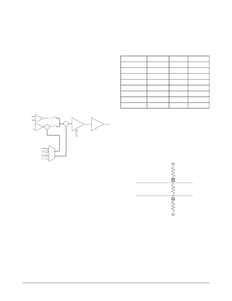
�Figure� 11.� Output� Structure�
�Figure� 11� shows� the� architecture� of� the� output� amplifier.�
�R� DAC_VHIGH�
�The� odd� and� even� column� amplifiers� sample� both� pixel� and�
�reset� value� to� perform� a� double� sampling� FPN� correction.�
�You� can� adjust� two� different� offsets� using� the� on-chip� DAC�
�(7� bit):� DAC_FINE� and� DAC_RAW.� DAC_FINE� is� used� to�
�tune� the� difference� between� odd� and� even� columns;�
�DAC_RAW� is� used� to� add� a� common� (both� even� and� odd�
�columns)� to� the� FPN� corrected� pixel� value.� This� pixel� value�
�is� fed� to� the� first� amplifier� stage� which� has� an� adjustable�
�DAC_VHIGH� =� 3.3V�
�R� DAC�
�DAC_VLOW� =� 0V�
�external�
�internal�
�7.88� k� W�
�internal�
�external�
�R� DAC_VLOW�
�gain,� controlled� by� a� 4-bit� word� (‘GAIN� [0� …� 3]’).�
�After� this,� a� unity� feedback� amplifier� buffers� the� signal�
�and� the� signal� leaves� the� chip.� This� second� amplifier� stage�
�determines� the� maximal� readout� speed,� that� is,� the�
�bandwidth� and� the� slew� rate� of� the� output� signal.� The� whole�
�amplifier� chain� is� designed� for� a� data� rate� of� 40� Mpix/s� (at�
�20� pF).�
�Figure� 12.� Internal� and� External� ADC� Connections�
�The� internal� resistor� R� DAC� has� a� value� of� approximately�
�7.88� k� W� .� The� recommend� resistor� values� for� both�
�DAC_VLOW� and� DAC_VHIGH� are� 0� W� .�
�The� analog� output� of� the� sensor� is� not� designed� to� drive�
�very� large� loads� on� the� PCB.� Therefore,� it� is� advised� that� the�
�PXL_OUT� is� connected� to� the� ADC_IN� right� below� the�
�sensor� in� the� top� layer� with� a� thick� track.� It� is� better� not� to�
�have� vias� on� this� trace.� If� there� is� a� socket� being� used,� then�
�it� is� advised� that� we� buffer� the� PXL_OUT� close� to� the� sensor�
�output� pin� and� then� take� the� signal� to� the� ADC_IN.�
�http://onsemi.com�
�12�
�相关PDF资料 |
PDF描述 |
|---|---|
| NOIL1SC4000A-GDC | IC IMAGE SENSOR 4MP 127-PGA |
| NOIL1SE3000A-GDC | IC IMAGE SENSOR 3MP 369-PGA |
| NOIL1SM0300A-WWC | IC IMAGE SENSOR LUPA300 48LLC |
| NOIL2SC1300A-GDC | IC IMAGE SENSOR LUPA1300 168PGA |
| NOIV1SE025KA-GDC | IC IMAGE SENSOR 25MP 355PGA |
相关代理商/技术参数 |
参数描述 |
|---|---|
| NOIL1SC4000A-GDC | 功能描述:IC IMAGE SENSOR 4MP 127-PGA RoHS:是 类别:传感器,转换器 >> 图像,相机 系列:* 标准包装:480 系列:- 象素大小:6.7µm x 6.7µm 有源象素阵列:768H x 488V 每秒帧数:52 电源电压:3.3V 类型:CMOS 成像 封装/外壳:48-QFP 供应商设备封装:48-QFP 包装:托盘 请注意:* 配用:4H2105-ND - HEADBOARD FOR KAC-004014H2104-ND - KIT EVAL FOR KAC-00401 其它名称:4H20954H2095-NDKAC-00401-CBC-LB-A0 |
| NOIL1SE0300A-QDC | 功能描述:SENSOR IMAGE COLOR CMOS 48-LCC RoHS:否 类别:传感器,转换器 >> 图像,相机 系列:- 标准包装:480 系列:- 象素大小:6.7µm x 6.7µm 有源象素阵列:768H x 488V 每秒帧数:52 电源电压:3.3V 类型:CMOS 成像 封装/外壳:48-QFP 供应商设备封装:48-QFP 包装:托盘 请注意:* 配用:4H2105-ND - HEADBOARD FOR KAC-004014H2104-ND - KIT EVAL FOR KAC-00401 其它名称:4H20954H2095-NDKAC-00401-CBC-LB-A0 |
| NOIL1SE3000A-GDC | 功能描述:IC IMAGE SENSOR 3MP 369-PGA RoHS:是 类别:传感器,转换器 >> 图像,相机 系列:* 标准包装:480 系列:- 象素大小:6.7µm x 6.7µm 有源象素阵列:768H x 488V 每秒帧数:52 电源电压:3.3V 类型:CMOS 成像 封装/外壳:48-QFP 供应商设备封装:48-QFP 包装:托盘 请注意:* 配用:4H2105-ND - HEADBOARD FOR KAC-004014H2104-ND - KIT EVAL FOR KAC-00401 其它名称:4H20954H2095-NDKAC-00401-CBC-LB-A0 |
| NOIL1SM0300A-QDC | 功能描述:IC IMAGE SENSOR LUPA300 48LLC RoHS:是 类别:传感器,转换器 >> 图像,相机 系列:* 标准包装:480 系列:- 象素大小:6.7µm x 6.7µm 有源象素阵列:768H x 488V 每秒帧数:52 电源电压:3.3V 类型:CMOS 成像 封装/外壳:48-QFP 供应商设备封装:48-QFP 包装:托盘 请注意:* 配用:4H2105-ND - HEADBOARD FOR KAC-004014H2104-ND - KIT EVAL FOR KAC-00401 其它名称:4H20954H2095-NDKAC-00401-CBC-LB-A0 |
| NOIL1SM0300A-WWC | 功能描述:IC IMAGE SENSOR LUPA300 48LLC RoHS:是 类别:传感器,转换器 >> 图像,相机 系列:LUPA300 标准包装:480 系列:- 象素大小:6.7µm x 6.7µm 有源象素阵列:768H x 488V 每秒帧数:52 电源电压:3.3V 类型:CMOS 成像 封装/外壳:48-QFP 供应商设备封装:48-QFP 包装:托盘 请注意:* 配用:4H2105-ND - HEADBOARD FOR KAC-004014H2104-ND - KIT EVAL FOR KAC-00401 其它名称:4H20954H2095-NDKAC-00401-CBC-LB-A0 |
发布紧急采购,3分钟左右您将得到回复。