- 您现在的位置:买卖IC网 > PDF目录224604 > NT511740D5J-5L (NANYA TECHNOLOGY CORP) 4M X 4 EDO DRAM, 50 ns, PDSO24 PDF资料下载
参数资料
| 型号: | NT511740D5J-5L |
| 厂商: | NANYA TECHNOLOGY CORP |
| 元件分类: | DRAM |
| 英文描述: | 4M X 4 EDO DRAM, 50 ns, PDSO24 |
| 封装: | 0.300 INCH, PLASTIC, SOJ-26/24 |
| 文件页数: | 13/16页 |
| 文件大小: | 129K |
| 代理商: | NT511740D5J-5L |
NT511740D5J
16MEG : x4
CMOS with Extended Data Out
REV 1.0 May. 2000
6
NANYA TECHNOLOGY CORP.
NAYNA TECHNOLOGY CORP. reserves the right to change products and specifications without notice.
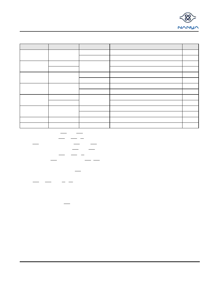
DC CHARACTERISTICS ( Continued )
Symbol
Power
Speed
Max
Units
-5
110
mA
ICC1
Don’t care
-6
100
mA
Normal
2
mA
ICC2
L
Don’t care
1
mA
-5
110
mA
ICC3
Don’t care
-6
100
mA
-5
90
mA
ICC4
Don’t care
-6
80
mA
Normal
3
mA
ICC5
L
Don’t care
200
uA
-5
110
mA
ICC6
Don’t care
-6
100
mA
ICC7
L
Don’t care
300
uA
ICCS
L
Don’t care
250
uA
ICC1* : Operating Current ( RAS and CAS cycling @ t RC=min.)
ICC2 : Standby Current ( RAS = CAS = W =VIH)
ICC3* : RAS -only Refresh Current ( RAS =VIH, RAS cycling @ t RC=min.)
ICC4* : Hyper Page Mode Current ( RAS =VIL, CAS Address cycling @ t HPC=min.)
ICC5 : Standby Current ( RAS = CAS
= W =VCC-0.2V)
ICC6* : CAS-Before- RAS Refresh Current ( RAS , CAS
cycling @ t RC=min.)
ICC7 : Battery back-up current, Average power supply current, Battery back-up mode Input high voltage (VIH)=VCC-0.2V,
Input low voltage (VIL)=0.2V, CAS =0.2V, DQ=Don’t care, t RC=125us(2K/L-ver) , t RAS=tRASmin~300ns
ICCS : Self Refresh Current
( RAS = CAS =0.2V, W = OE =A0 ~ A11=VCC-0.2V or 0.2V, DQ0 ~ DQ3=VCC-0.2V, 0.2V or open )
*Note : ICC1, ICC3, ICC4 and ICC6 are dependent on output loading and cycle rates. Specified values are obtained with
the output open. ICC is specified as an average current. In ICC1, ICC3 and ICC6, address can be changed
maximum once while RAS =VIL. In ICC4, address can be changed maximum once within one hyper page mode
cycle time, t HPC.
相关PDF资料 |
PDF描述 |
|---|---|
| NT5SV8M16FT-75BI | 8M X 16 SYNCHRONOUS DRAM, 5.4 ns, PDSO54 |
| NT5TU64M16DG-3C | 64M X 16 DDR DRAM, 0.45 ns, PBGA84 |
| NTA2425E | |
| NTA2425F | |
| NTA2410-10 | |
相关代理商/技术参数 |
参数描述 |
|---|---|
| NT511740D5J-60 | 制造商:未知厂家 制造商全称:未知厂家 功能描述:CMOS with Extended Data Out |
| NT511740D5J-6L | 制造商:未知厂家 制造商全称:未知厂家 功能描述:CMOS with Extended Data Out |
| NT512D64S8HB0G | 制造商:未知厂家 制造商全称:未知厂家 功能描述:184 pin Unbuffered DDR DIMM |
| NT512D64S8HB0G-75B | 制造商:未知厂家 制造商全称:未知厂家 功能描述:184 pin Unbuffered DDR DIMM |
| NT512D64S8HB1G | 制造商:未知厂家 制造商全称:未知厂家 功能描述:184 pin Unbuffered DDR DIMM |
发布紧急采购,3分钟左右您将得到回复。