- 您现在的位置:买卖IC网 > PDF目录18006 > NTB5404NT4G (ON Semiconductor)MOSFET N-CH 40V 136A D2PAK PDF资料下载
参数资料
| 型号: | NTB5404NT4G |
| 厂商: | ON Semiconductor |
| 文件页数: | 1/7页 |
| 文件大小: | 0K |
| 描述: | MOSFET N-CH 40V 136A D2PAK |
| 产品变化通告: | Reactivation Notice 08/Apr/2011 Product Obsolescence 24/Jan/2011 |
| 标准包装: | 800 |
| FET 型: | MOSFET N 通道,金属氧化物 |
| FET 特点: | 标准 |
| 漏极至源极电压(Vdss): | 40V |
| 电流 - 连续漏极(Id) @ 25° C: | 136A |
| 开态Rds(最大)@ Id, Vgs @ 25° C: | 4.5 毫欧 @ 40A,10V |
| Id 时的 Vgs(th)(最大): | 4V @ 250µA |
| 闸电荷(Qg) @ Vgs: | 125nC @ 10V |
| 输入电容 (Ciss) @ Vds: | 7000pF @ 32V |
| 功率 - 最大: | 167W |
| 安装类型: | 表面贴装 |
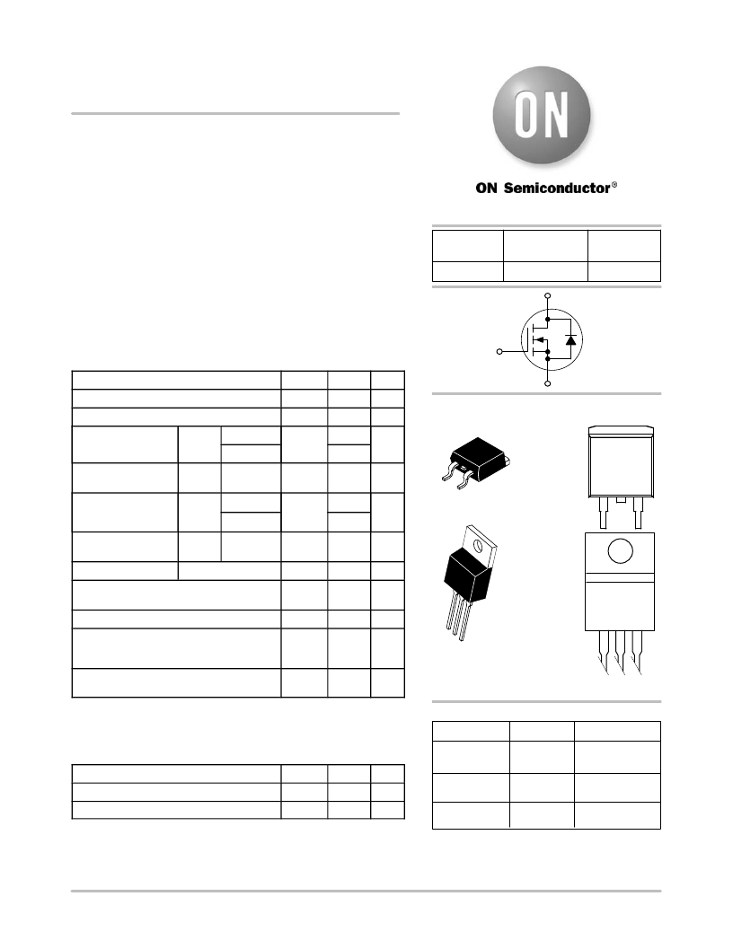
| 封装/外壳: | TO-263-3,D²Pak(2 引线+接片),TO-263AB |
| 供应商设备封装: | D2PAK |
| 包装: | 带卷 (TR) |
�� �
�
�NTB5404N,� NTP5404N,�
�NVB5404N�
�Power� MOSFET�
�40� V,� 167� A,� Single� N� ?� Channel,� D� 2� PAK� &�
�TO� ?� 220�
�Features�
�?� Low� R� DS(on)�
�?� High� Current� Capability�
�?� Low� Gate� Charge�
�?� AEC� ?� Q101� Qualified� and� PPAP� Capable� ?� NVB5404N�
�?� These� Devices� are� Pb� ?� Free� and� are� RoHS� Compliant�
�Applications�
�?� Electronic� Brake� Systems�
�?� Electronic� Power� Steering�
�?� Bridge� Circuits�
�MAXIMUM� RATINGS� (T� J� =� 25� °� C� unless� otherwise� stated)�
�V� (BR)DSS�
�40� V�
�N� ?� Channel�
�G�
�http://onsemi.com�
�R� DS(ON)� MAX�
�4.5� m� W� @� 10� V�
�D�
�I� D� MAX�
�(Note� 1)�
�167� A�
�Parameter�
�Drain� ?� to� ?� Source� Voltage�
�Gate� ?� to� ?� Source� Voltage�
�Symbol�
�V� DSS�
�V� GS�
�Value�
�40�
�±� 20�
�Units�
�V�
�V�
�S�
�MARKING�
�D� IAGRAM� S�
�Continuous� Drain�
�Current� ?� R� q� JC�
�Power� Dissipation� ?�
�R� q� JC�
�Continuous� Drain�
�Current� ?� R� q� JA�
�(Note� 1)�
�Power� Dissipation� ?�
�R� q� JA� (Note� 1)�
�Steady�
�State�
�Steady�
�State�
�Steady�
�State�
�Steady�
�State�
�T� C� =� 25� °� C�
�T� C� =� 100� °� C�
�T� C� =� 25� °� C�
�T� A� =� 25� °� C�
�T� A� =� 100� °� C�
�T� A� =� 25� °� C�
�I� D�
�P� D�
�I� D�
�P� D�
�167�
�118�
�254�
�24�
�17�
�5.4�
�A�
�W�
�A�
�W�
�1�
�2�
�3�
�4�
�D� 2� PAK�
�CASE� 418B�
�STYLE� 2�
�NTB5404NG�
�AYWW�
�1�
�Pulsed� Drain� Current� t� p� =� 10� m� s�
�Operating� Junction� and� Storage� Temperature�
�Source� Current� (Body� Diode)� Pulsed�
�I� DM�
�T� J� ,�
�T� STG�
�I� S�
�670�
�?� 55� to�
�175�
�75�
�A�
�°� C�
�A�
�TO� ?� 220AB�
�CASE� 221A�
�STYLE� 5�
�NTP5404NRG�
�AYWW�
�Single� Pulse� Drain� ?� to� Source� Avalanche�
�Energy� ?� (V� DD� =� 50� V,� V� GS� =� 10� V,� I� PK� =� 45� A,�
�L� =� 1� mH,� R� G� =� 25� W� )�
�Lead� Temperature� for� Soldering� Purposes�
�(1/8”� from� case� for� 10� s)�
�EAS�
�T� L�
�1000�
�260�
�mJ�
�°� C�
�1�
�2�
�3�
�G�
�A�
�Y�
�WW�
�=� Pb� ?� Free� Device�
�=� Assembly� Location�
�=� Year�
�=� Work� Week�
�Stresses� exceeding� Maximum� Ratings� may� damage� the� device.� Maximum�
�Ratings� are� stress� ratings� only.� Functional� operation� above� the� Recommended�
�Operating� Conditions� is� not� implied.� Extended� exposure� to� stresses� above� the�
�Recommended� Operating� Conditions� may� affect� device� reliability.�
�ORDERING� INFORMATION�
�Device� Package� Shipping� ?�
�THERMAL� RESISTANCE� RATINGS�
�Parameter�
�Junction� ?� to� ?� Case� (Drain)�
�Symbol�
�R� θ� JC�
�Max�
�0.59�
�Unit�
�°� C/W�
�NTB5404NT4G�
�NTP5404NRG�
�D� 2� PAK�
�(Pb� ?� Free)�
�TO� ?� 220�
�(Pb� ?� Free)�
�800� /� Tape� &� Reel�
�50� Units� /� Rail�
�Junction� ?� to� ?� Ambient� (Note� 1)� R� θ� JA�
�1.� Surface� mounted� on� FR4� board� using� 1� sq� in� pad� size,�
�(Cu� Area� 1.127� sq� in� [2� oz]� including� traces).�
�?� Semiconductor� Components� Industries,� LLC,� 2012�
�June,� 2012� ?� Rev.� 7�
�50�
�1�
�°� C/W�
�NVB5404NT4G� D� 2� PAK� 800� /� Tape� &� Reel�
�(Pb� ?� Free)�
�?For� information� on� tape� and� reel� specifications,�
�including� part� orientation� and� tape� sizes,� please�
�refer� to� our� Tape� and� Reel� Packaging� Specifications�
�Brochure,� BRD8011/D.�
�Publication� Order� Number:�
�NTB5404N/D�
�相关PDF资料 |
PDF描述 |
|---|---|
| MC08CA020C-F | CAP MICA 2PF 100V 0805 |
| CD6ED500JO3 | CAP MICA 50PF 500V 5% RADIAL |
| CD15FD151FO3 | CAP MICA 150PF 500V 1% RADIAL |
| PDA620003 | OSC 106.25MHZ 3.3V SMD |
| CD5EC300GO3F | CAP MICA 30PF 300V 2% RADIAL |
相关代理商/技术参数 |
参数描述 |
|---|---|
| NTB5405N | 制造商:ONSEMI 制造商全称:ON Semiconductor 功能描述:Power MOSFET 40 V, 116 A, Single N−Channel, D2PAK |
| NTB5405NG | 功能描述:MOSFET NFET 40V 116A PB RoHS:否 制造商:STMicroelectronics 晶体管极性:N-Channel 汲极/源极击穿电压:650 V 闸/源击穿电压:25 V 漏极连续电流:130 A 电阻汲极/源极 RDS(导通):0.014 Ohms 配置:Single 最大工作温度: 安装风格:Through Hole 封装 / 箱体:Max247 封装:Tube |
| NTB5405NT4G | 功能描述:MOSFET NFET 40V 116A PB RoHS:否 制造商:STMicroelectronics 晶体管极性:N-Channel 汲极/源极击穿电压:650 V 闸/源击穿电压:25 V 漏极连续电流:130 A 电阻汲极/源极 RDS(导通):0.014 Ohms 配置:Single 最大工作温度: 安装风格:Through Hole 封装 / 箱体:Max247 封装:Tube |
| NTB5411N | 制造商:ONSEMI 制造商全称:ON Semiconductor 功能描述:Power MOSFET 80 Amps, 60 Volts N-Channel D2PAK, TO-220 |
| NTB5411NT4G | 功能描述:MOSFET NFET D2PAK 60V 75A 12.5mOhm RoHS:否 制造商:STMicroelectronics 晶体管极性:N-Channel 汲极/源极击穿电压:650 V 闸/源击穿电压:25 V 漏极连续电流:130 A 电阻汲极/源极 RDS(导通):0.014 Ohms 配置:Single 最大工作温度: 安装风格:Through Hole 封装 / 箱体:Max247 封装:Tube |
发布紧急采购,3分钟左右您将得到回复。