- 您现在的位置:买卖IC网 > PDF目录18006 > NTB5404NT4G (ON Semiconductor)MOSFET N-CH 40V 136A D2PAK PDF资料下载
参数资料
| 型号: | NTB5404NT4G |
| 厂商: | ON Semiconductor |
| 文件页数: | 7/7页 |
| 文件大小: | 0K |
| 描述: | MOSFET N-CH 40V 136A D2PAK |
| 产品变化通告: | Reactivation Notice 08/Apr/2011 Product Obsolescence 24/Jan/2011 |
| 标准包装: | 800 |
| FET 型: | MOSFET N 通道,金属氧化物 |
| FET 特点: | 标准 |
| 漏极至源极电压(Vdss): | 40V |
| 电流 - 连续漏极(Id) @ 25° C: | 136A |
| 开态Rds(最大)@ Id, Vgs @ 25° C: | 4.5 毫欧 @ 40A,10V |
| Id 时的 Vgs(th)(最大): | 4V @ 250µA |
| 闸电荷(Qg) @ Vgs: | 125nC @ 10V |
| 输入电容 (Ciss) @ Vds: | 7000pF @ 32V |
| 功率 - 最大: | 167W |
| 安装类型: | 表面贴装 |
| 封装/外壳: | TO-263-3,D²Pak(2 引线+接片),TO-263AB |
| 供应商设备封装: | D2PAK |
| 包装: | 带卷 (TR) |
�� �
�
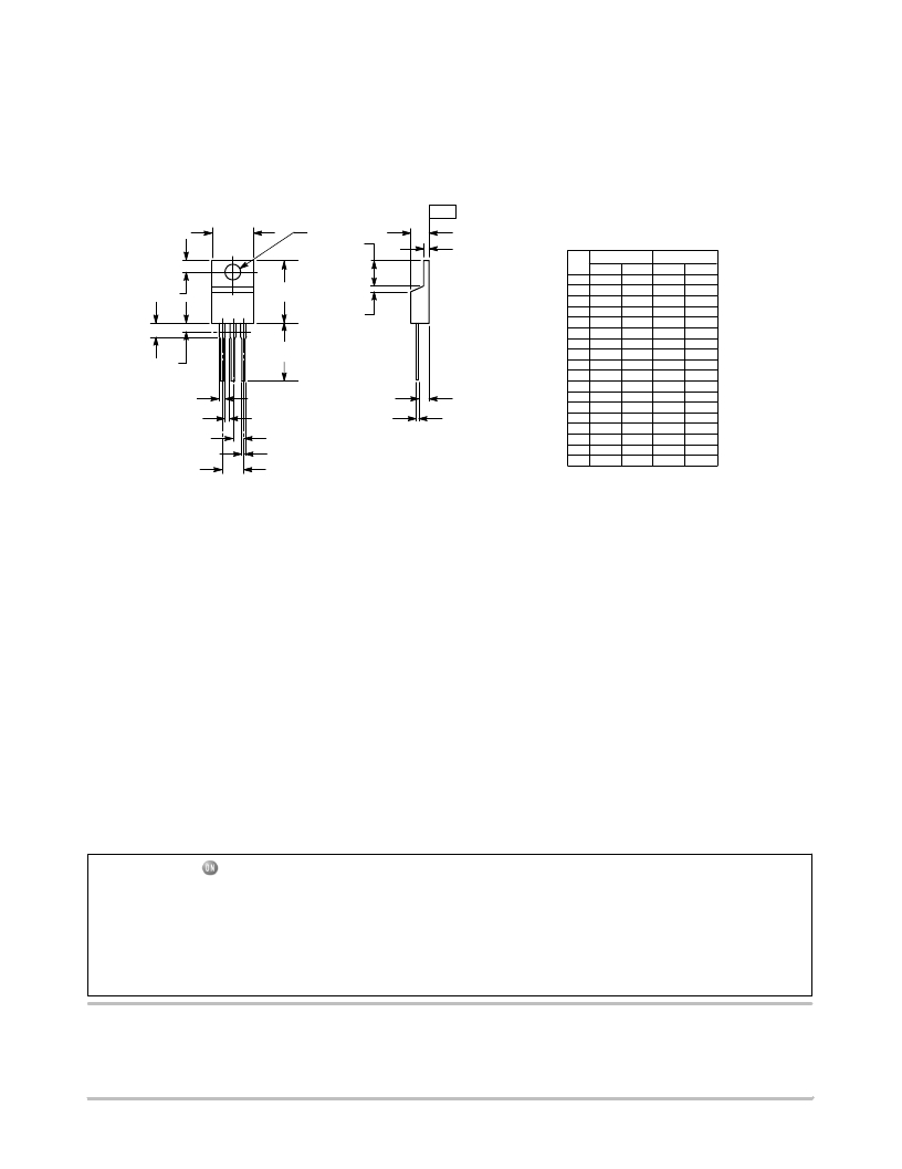
�NTB5404N,� NTP5404N,� NVB5404N�
�PACKAGE� DIMENSIONS�
�TO� ?� 220�
�CASE� 221A� ?� 09�
�ISSUE� AG�
�NOTES:�
�1.� DIMENSIONING� AND� TOLERANCING� PER� ANSI�
�B�
�F�
�T�
�S�
�C�
�?� T� ?�
�SEATING�
�PLANE�
�Y14.5M,� 1982.�
�2.� CONTROLLING� DIMENSION:� INCH.�
�3.� DIMENSION� Z� DEFINES� A� ZONE� WHERE� ALL�
�BODY� AND� LEAD� IRREGULARITIES� ARE�
�ALLOWED.�
�4�
�DIM�
�INCHES�
�MIN� MAX�
�MILLIMETERS�
�MIN� MAX�
�Q�
�A�
�A�
�B�
�C�
�0.570� 0.620�
�0.380� 0.405�
�0.160� 0.190�
�14.48� 15.75�
�9.66� 10.28�
�4.07� 4.82�
�H�
�Z�
�1� 2� 3�
�K�
�U�
�D�
�F�
�G�
�H�
�J�
�K�
�0.025� 0.036�
�0.142� 0.161�
�0.095� 0.105�
�0.110� 0.161�
�0.014� 0.025�
�0.500� 0.562�
�0.64� 0.91�
�3.61� 4.09�
�2.42� 2.66�
�2.80� 4.10�
�0.36� 0.64�
�12.70� 14.27�
�L�
�0.045� 0.060�
�1.15� 1.52�
�L�
�V�
�G�
�R�
�J�
�N�
�Q�
�R�
�S�
�T�
�U�
�0.190� 0.210�
�0.100� 0.120�
�0.080� 0.110�
�0.045� 0.055�
�0.235� 0.255�
�0.000� 0.050�
�4.83� 5.33�
�2.54� 3.04�
�2.04� 2.79�
�1.15� 1.39�
�5.97� 6.47�
�0.00� 1.27�
�N�
�D�
�V� 0.045� ---�
�Z� ---� 0.080�
�STYLE� 5:�
�PIN� 1.�
�2.�
�3.�
�4.�
�GATE�
�DRAIN�
�SOURCE�
�DRAIN�
�1.15� ---�
�---� 2.04�
�ON� Semiconductor� and� are� registered� trademarks� of� Semiconductor� Components� Industries,� LLC� (SCILLC).� SCILLC� owns� the� rights� to� a� number� of� patents,� trademarks,�
�copyrights,� trade� secrets,� and� other� intellectual� property.� A� listing� of� SCILLC’s� product/patent� coverage� may� be� accessed� at� www.onsemi.com/site/pdf/Patent� ?� Marking.pdf.� SCILLC�
�reserves� the� right� to� make� changes� without� further� notice� to� any� products� herein.� SCILLC� makes� no� warranty,� representation� or� guarantee� regarding� the� suitability� of� its� products� for� any�
�particular� purpose,� nor� does� SCILLC� assume� any� liability� arising� out� of� the� application� or� use� of� any� product� or� circuit,� and� specifically� disclaims� any� and� all� liability,� including� without�
�limitation� special,� consequential� or� incidental� damages.� “Typical”� parameters� which� may� be� provided� in� SCILLC� data� sheets� and/or� specifications� can� and� do� vary� in� different� applications�
�and� actual� performance� may� vary� over� time.� All� operating� parameters,� including� “Typicals”� must� be� validated� for� each� customer� application� by� customer’s� technical� experts.� SCILLC�
�does� not� convey� any� license� under� its� patent� rights� nor� the� rights� of� others.� SCILLC� products� are� not� designed,� intended,� or� authorized� for� use� as� components� in� systems� intended� for�
�surgical� implant� into� the� body,� or� other� applications� intended� to� support� or� sustain� life,� or� for� any� other� application� in� which� the� failure� of� the� SCILLC� product� could� create� a� situation� where�
�personal� injury� or� death� may� occur.� Should� Buyer� purchase� or� use� SCILLC� products� for� any� such� unintended� or� unauthorized� application,� Buyer� shall� indemnify� and� hold� SCILLC� and�
�its� officers,� employees,� subsidiaries,� affiliates,� and� distributors� harmless� against� all� claims,� costs,� damages,� and� expenses,� and� reasonable� attorney� fees� arising� out� of,� directly� or� indirectly,�
�any� claim� of� personal� injury� or� death� associated� with� such� unintended� or� unauthorized� use,� even� if� such� claim� alleges� that� SCILLC� was� negligent� regarding� the� design� or� manufacture�
�of� the� part.� SCILLC� is� an� Equal� Opportunity/Affirmative� Action� Employer.� This� literature� is� subject� to� all� applicable� copyright� laws� and� is� not� for� resale� in� any� manner.�
�PUBLICATION� ORDERING� INFORMATION�
�LITERATURE� FULFILLMENT� :�
�Literature� Distribution� Center� for� ON� Semiconductor�
�P.O.� Box� 5163,� Denver,� Colorado� 80217� USA�
�Phone� :� 303� ?� 675� ?� 2175� or� 800� ?� 344� ?� 3860� Toll� Free� USA/Canada�
�Fax� :� 303� ?� 675� ?� 2176� or� 800� ?� 344� ?� 3867� Toll� Free� USA/Canada�
�Email� :� orderlit@onsemi.com�
�N.� American� Technical� Support� :� 800� ?� 282� ?� 9855� Toll� Free�
�USA/Canada�
�Europe,� Middle� East� and� Africa� Technical� Support:�
�Phone:� 421� 33� 790� 2910�
�Japan� Customer� Focus� Center�
�Phone:� 81� ?� 3� ?� 5817� ?� 1050�
�http://onsemi.com�
�7�
�ON� Semiconductor� Website� :� www.onsemi.com�
�Order� Literature� :� http://www.onsemi.com/orderlit�
�For� additional� information,� please� contact� your� local�
�Sales� Representative�
�NTB5404N/D�
�相关PDF资料 |
PDF描述 |
|---|---|
| MC08CA020C-F | CAP MICA 2PF 100V 0805 |
| CD6ED500JO3 | CAP MICA 50PF 500V 5% RADIAL |
| CD15FD151FO3 | CAP MICA 150PF 500V 1% RADIAL |
| PDA620003 | OSC 106.25MHZ 3.3V SMD |
| CD5EC300GO3F | CAP MICA 30PF 300V 2% RADIAL |
相关代理商/技术参数 |
参数描述 |
|---|---|
| NTB5405N | 制造商:ONSEMI 制造商全称:ON Semiconductor 功能描述:Power MOSFET 40 V, 116 A, Single N−Channel, D2PAK |
| NTB5405NG | 功能描述:MOSFET NFET 40V 116A PB RoHS:否 制造商:STMicroelectronics 晶体管极性:N-Channel 汲极/源极击穿电压:650 V 闸/源击穿电压:25 V 漏极连续电流:130 A 电阻汲极/源极 RDS(导通):0.014 Ohms 配置:Single 最大工作温度: 安装风格:Through Hole 封装 / 箱体:Max247 封装:Tube |
| NTB5405NT4G | 功能描述:MOSFET NFET 40V 116A PB RoHS:否 制造商:STMicroelectronics 晶体管极性:N-Channel 汲极/源极击穿电压:650 V 闸/源击穿电压:25 V 漏极连续电流:130 A 电阻汲极/源极 RDS(导通):0.014 Ohms 配置:Single 最大工作温度: 安装风格:Through Hole 封装 / 箱体:Max247 封装:Tube |
| NTB5411N | 制造商:ONSEMI 制造商全称:ON Semiconductor 功能描述:Power MOSFET 80 Amps, 60 Volts N-Channel D2PAK, TO-220 |
| NTB5411NT4G | 功能描述:MOSFET NFET D2PAK 60V 75A 12.5mOhm RoHS:否 制造商:STMicroelectronics 晶体管极性:N-Channel 汲极/源极击穿电压:650 V 闸/源击穿电压:25 V 漏极连续电流:130 A 电阻汲极/源极 RDS(导通):0.014 Ohms 配置:Single 最大工作温度: 安装风格:Through Hole 封装 / 箱体:Max247 封装:Tube |
发布紧急采购,3分钟左右您将得到回复。