- 您现在的位置:买卖IC网 > Datasheet目录489 > NTK3134NT5G (ON Semiconductor)MOSFET N-CH 20V 750MA SOT-723 Datasheet资料下载
参数资料
| 型号: | NTK3134NT5G |
| 厂商: | ON Semiconductor |
| 文件页数: | 5/5页 |
| 文件大小: | 0K |
| 描述: | MOSFET N-CH 20V 750MA SOT-723 |
| 产品变化通告: | 1Q2012 Discontinuation 30/Mar/2012 |
| 标准包装: | 8,000 |
| FET 型: | MOSFET N 通道,金属氧化物 |
| FET 特点: | 逻辑电平门 |
| 漏极至源极电压(Vdss): | 20V |
| 电流 - 连续漏极(Id) @ 25° C: | 750mA |
| 开态Rds(最大)@ Id, Vgs @ 25° C: | 350 毫欧 @ 890mA,4.5V |
| Id 时的 Vgs(th)(最大): | 1.2V @ 250µA |
| 输入电容 (Ciss) @ Vds: | 120pF @ 16V |
| 功率 - 最大: | 310mW |
| 安装类型: | 表面贴装 |
| 封装/外壳: | SOT-723 |
| 供应商设备封装: | SOT-723 |
| 包装: | 带卷 (TR) |
��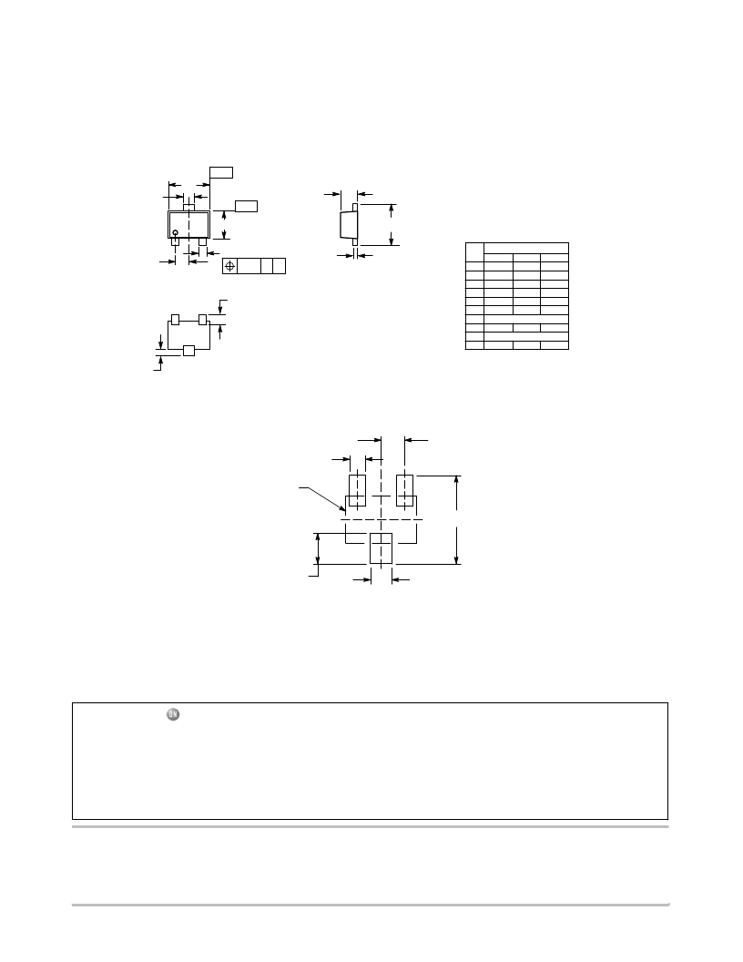 �
�
�NTK3134N�
�PACKAGE� DIMENSIONS�
�SOT� ?� 723�
�CASE� 631AA�
�ISSUE� D�
�2X�
�b1�
�e�
�?� X� ?�
�D�
�E�
�1� 2�
�TOP� VIEW�
�1�
�3� ?� Y� ?�
�2X� b�
�0.08� X� Y�
�3X� L�
�A�
�C�
�SIDE� VIEW�
�H� E�
�NOTES:�
�1.� DIMENSIONING� AND� TOLERANCING� PER� ASME�
�Y14.5M,� 1994.�
�2.� CONTROLLING� DIMENSION:� MILLIMETERS.�
�3.� MAXIMUM� LEAD� THICKNESS� INCLUDES� LEAD�
�FINISH.� MINIMUM� LEAD� THICKNESS� IS� THE� MINIMUM�
�THICKNESS� OF� BASE� MATERIAL.�
�4.� DIMENSIONS� D� AND� E� DO� NOT� INCLUDE� MOLD�
�FLASH,� PROTRUSIONS� OR� GATE� BURRS.�
�MILLIMETERS�
�DIM� MIN� NOM� MAX�
�A� 0.45� 0.50� 0.55�
�b� 0.15� 0.21� 0.27�
�b1� 0.25� 0.31� 0.37�
�C� 0.07� 0.12� 0.17�
�D� 1.15� 1.20� 1.25�
�E� 0.75� 0.80� 0.85�
�e� 0.40� BSC�
�H� E� 1.15� 1.20� 1.25�
�L� 0.29� REF�
�L2� 0.15� 0.20� 0.25�
�3X�
�L2�
�BOTTOM� VIEW�
�RECOMMENDED�
�SOLDERING� FOOTPRINT*�
�STYLE� 5:�
�PIN� 1.� GATE�
�2.� SOURCE�
�3.� DRAIN�
�2X�
�0.40�
�2X�
�0.27�
�PACKAGE�
�OUTLINE�
�1.50�
�3X�
�0.52�
�0.36�
�DIMENSIONS:� MILLIMETERS�
�*For� additional� information� on� our� Pb� ?� Free� strategy� and� soldering�
�details,� please� download� the� ON� Semiconductor� Soldering� and�
�Mounting� Techniques� Reference� Manual,� SOLDERRM/D.�
�ON� Semiconductor� and� are� registered� trademarks� of� Semiconductor� Components� Industries,� LLC� (SCILLC).� SCILLC� owns� the� rights� to� a� number� of� patents,� trademarks,�
�copyrights,� trade� secrets,� and� other� intellectual� property.� A� listing� of� SCILLC’s� product/patent� coverage� may� be� accessed� at� www.onsemi.com/site/pdf/Patent� ?� Marking.pdf.� SCILLC�
�reserves� the� right� to� make� changes� without� further� notice� to� any� products� herein.� SCILLC� makes� no� warranty,� representation� or� guarantee� regarding� the� suitability� of� its� products� for� any�
�particular� purpose,� nor� does� SCILLC� assume� any� liability� arising� out� of� the� application� or� use� of� any� product� or� circuit,� and� specifically� disclaims� any� and� all� liability,� including� without�
�limitation� special,� consequential� or� incidental� damages.� “Typical”� parameters� which� may� be� provided� in� SCILLC� data� sheets� and/or� specifications� can� and� do� vary� in� different� applications�
�and� actual� performance� may� vary� over� time.� All� operating� parameters,� including� “Typicals”� must� be� validated� for� each� customer� application� by� customer’s� technical� experts.� SCILLC�
�does� not� convey� any� license� under� its� patent� rights� nor� the� rights� of� others.� SCILLC� products� are� not� designed,� intended,� or� authorized� for� use� as� components� in� systems� intended� for�
�surgical� implant� into� the� body,� or� other� applications� intended� to� support� or� sustain� life,� or� for� any� other� application� in� which� the� failure� of� the� SCILLC� product� could� create� a� situation� where�
�personal� injury� or� death� may� occur.� Should� Buyer� purchase� or� use� SCILLC� products� for� any� such� unintended� or� unauthorized� application,� Buyer� shall� indemnify� and� hold� SCILLC� and�
�its� officers,� employees,� subsidiaries,� affiliates,� and� distributors� harmless� against� all� claims,� costs,� damages,� and� expenses,� and� reasonable� attorney� fees� arising� out� of,� directly� or� indirectly,�
�any� claim� of� personal� injury� or� death� associated� with� such� unintended� or� unauthorized� use,� even� if� such� claim� alleges� that� SCILLC� was� negligent� regarding� the� design� or� manufacture�
�of� the� part.� SCILLC� is� an� Equal� Opportunity/Affirmative� Action� Employer.� This� literature� is� subject� to� all� applicable� copyright� laws� and� is� not� for� resale� in� any� manner.�
�PUBLICATION� ORDERING� INFORMATION�
�LITERATURE� FULFILLMENT� :�
�Literature� Distribution� Center� for� ON� Semiconductor�
�P.O.� Box� 5163,� Denver,� Colorado� 80217� USA�
�Phone� :� 303� ?� 675� ?� 2175� or� 800� ?� 344� ?� 3860� Toll� Free� USA/Canada�
�Fax� :� 303� ?� 675� ?� 2176� or� 800� ?� 344� ?� 3867� Toll� Free� USA/Canada�
�Email� :� orderlit@onsemi.com�
�N.� American� Technical� Support� :� 800� ?� 282� ?� 9855� Toll� Free�
�USA/Canada�
�Europe,� Middle� East� and� Africa� Technical� Support:�
�Phone:� 421� 33� 790� 2910�
�Japan� Customer� Focus� Center�
�Phone:� 81� ?� 3� ?� 5817� ?� 1050�
�http://onsemi.com�
�5�
�ON� Semiconductor� Website� :� www.onsemi.com�
�Order� Literature� :� http://www.onsemi.com/orderlit�
�For� additional� information,� please� contact� your� local�
�Sales� Representative�
�NTK3134N/D�
�相关PDF资料 |
PDF描述 |
|---|---|
| NTK3139PT5G | MOSFET P-CH 20V 660MA SOT-723 |
| NTK3142PT1G | MOSFET P-CHAN 260MA 20V SOT-723 |
| NTLGD3502NT2G | MOSFET N-CH DUAL 20V 6-DFN |
| NTLGF3402PT2G | MOSFET P-CH 20V 2.3A 6-DFN |
| NTLJD2104PTBG | MOSFET P-CH DUAL 12V 4.3A 6WDFN |
相关代理商/技术参数 |
参数描述 |
|---|---|
| NTK3134NT5H | 功能描述:MOSFET RoHS:否 制造商:STMicroelectronics 晶体管极性:N-Channel 汲极/源极击穿电压:650 V 闸/源击穿电压:25 V 漏极连续电流:130 A 电阻汲极/源极 RDS(导通):0.014 Ohms 配置:Single 最大工作温度: 安装风格:Through Hole 封装 / 箱体:Max247 封装:Tube |
| NTK3139P | 制造商:ONSEMI 制造商全称:ON Semiconductor 功能描述:Power MOSFET −20 V, −780 mA, Single P−Channel with ESD Protection, SOT−723 |
| NTK3139PT1G | 功能描述:MOSFET 20V/6V P CH T1 780mA 0.4 RoHS:否 制造商:STMicroelectronics 晶体管极性:N-Channel 汲极/源极击穿电压:650 V 闸/源击穿电压:25 V 漏极连续电流:130 A 电阻汲极/源极 RDS(导通):0.014 Ohms 配置:Single 最大工作温度: 安装风格:Through Hole 封装 / 箱体:Max247 封装:Tube |
| NTK3139PT1H | 制造商:Rochester Electronics LLC 功能描述: 制造商:ON Semiconductor 功能描述: |
| NTK3139PT5G | 功能描述:MOSFET 20V/6V P CH T1 780mA 0.4 RoHS:否 制造商:STMicroelectronics 晶体管极性:N-Channel 汲极/源极击穿电压:650 V 闸/源击穿电压:25 V 漏极连续电流:130 A 电阻汲极/源极 RDS(导通):0.014 Ohms 配置:Single 最大工作温度: 安装风格:Through Hole 封装 / 箱体:Max247 封装:Tube |
发布紧急采购,3分钟左右您将得到回复。