- 您现在的位置:买卖IC网 > PDF目录11733 > ORSO82G5-3FN680C (Lattice Semiconductor Corporation)IC TRANCEIVERS FPSC 680FPBGA PDF资料下载
参数资料
| 型号: | ORSO82G5-3FN680C |
| 厂商: | Lattice Semiconductor Corporation |
| 文件页数: | 79/153页 |
| 文件大小: | 0K |
| 描述: | IC TRANCEIVERS FPSC 680FPBGA |
| 产品变化通告: | Product Discontinuation 01/Aug/2011 |
| 标准包装: | 24 |
| 系列: | * |
第1页第2页第3页第4页第5页第6页第7页第8页第9页第10页第11页第12页第13页第14页第15页第16页第17页第18页第19页第20页第21页第22页第23页第24页第25页第26页第27页第28页第29页第30页第31页第32页第33页第34页第35页第36页第37页第38页第39页第40页第41页第42页第43页第44页第45页第46页第47页第48页第49页第50页第51页第52页第53页第54页第55页第56页第57页第58页第59页第60页第61页第62页第63页第64页第65页第66页第67页第68页第69页第70页第71页第72页第73页第74页第75页第76页第77页第78页当前第79页第80页第81页第82页第83页第84页第85页第86页第87页第88页第89页第90页第91页第92页第93页第94页第95页第96页第97页第98页第99页第100页第101页第102页第103页第104页第105页第106页第107页第108页第109页第110页第111页第112页第113页第114页第115页第116页第117页第118页第119页第120页第121页第122页第123页第124页第125页第126页第127页第128页第129页第130页第131页第132页第133页第134页第135页第136页第137页第138页第139页第140页第141页第142页第143页第144页第145页第146页第147页第148页第149页第150页第151页第152页第153页
Lattice Semiconductor
ORCA ORSO42G5 and ORSO82G5 Data Sheet
31
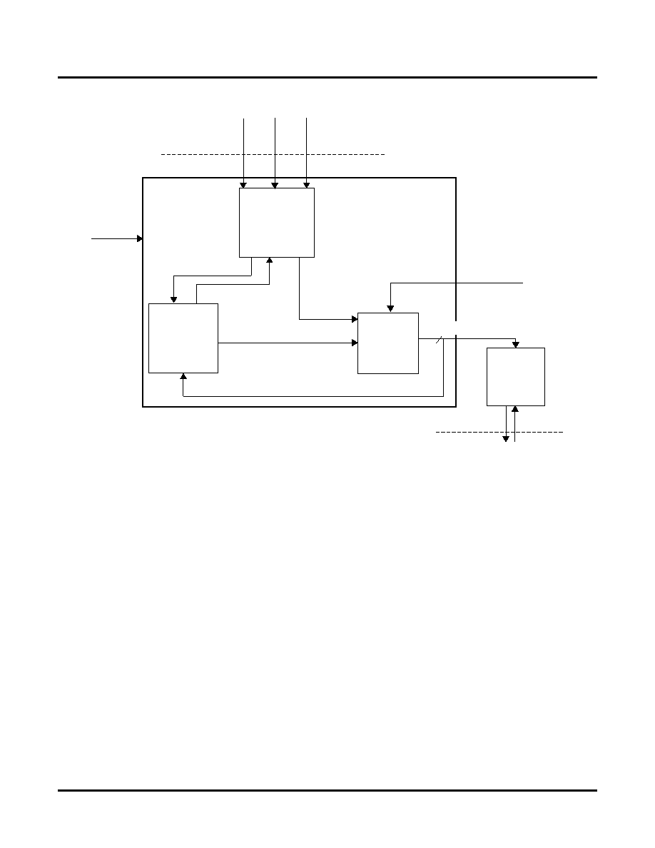
Figure 16. TX Frame Processor (TFP) Block Diagram
Payload Sub-block
The Payload sub block is activated by the cell mode frame pulse (cell mode) or DINxx_FP from FPGA (SONET
mode). A pulse on this signal indicates the start of a frame.
In SONET mode, only two types of data bytes are in each frame:
TOH bytes
SPE data bytes
There are N x 3 (N = 48) bytes of TOH per row and there are a total of 9 rows in a SONET frame. The rest of the
bytes in each row are SPE data bytes in SONET mode.
TOH Sub-block
This block is responsible formatting the 144 (48 x 3) bytes of TOH at the beginning of each row of the transport
frame. All TOH bytes may be transmitted transparently from the FPGA logic using the transparent mode. Alter-
nately, some or all TOH bytes may be inserted by the TOH block (AUTO_SOH and AUTO_TOH mode). The TOH
data is transferred across the FPGA/core interface as 32-bit words, hence 36 clock cycles (12 x 3) are needed to
transfer a TOH row. TOH insertion is controlled by software register bits as shown in the Register Map tables.
MUX
BLOCK
LDIN(7:0)
XCK311
PAYLOAD
BLOCK
TRANSPORT
OVERHEAD
BLOCK
SCRAMBLE
LOGIC
32-bit payload
scramble_disable
TX_FRM_PROC
SERDES INTERFACE
FPGA INTERFACE
(SONET MODE)
32-bit TOH data
Error
injection
controls
(control
register
bits)
Cell Mode
Frame Pulse
DINxy_FP
scramble_out (31:0)
DINxy[31:0] data
相关PDF资料 |
PDF描述 |
|---|---|
| PIC32MX675F256L-80I/PT | IC MCU 32BIT 256KB FLASH 100TQFP |
| D38999/26FE26SC | CONN PLUG 26POS STRAIGHT W/SCKT |
| MSP430F4783IPZ | IC MCU 16BIT 48KB FLASH 100LQFP |
| MS27656T17F99S | CONN RCPT 23POS WALL MNT W/SCKT |
| VI-J4B-IW-F3 | CONVERTER MOD DC/DC 95V 100W |
相关代理商/技术参数 |
参数描述 |
|---|---|
| ORSO82G5-3FN680C1 | 功能描述:FPGA - 现场可编程门阵列 10368 LUT 372 I/O RoHS:否 制造商:Altera Corporation 系列:Cyclone V E 栅极数量: 逻辑块数量:943 内嵌式块RAM - EBR:1956 kbit 输入/输出端数量:128 最大工作频率:800 MHz 工作电源电压:1.1 V 最大工作温度:+ 70 C 安装风格:SMD/SMT 封装 / 箱体:FBGA-256 |
| ORSO82G5-G2-PAC-EV | 功能描述:可编程逻辑 IC 开发工具 ORCA ORSO82G5-FPSC Eval Brd RoHS:否 制造商:Altera Corporation 产品:Development Kits 类型:FPGA 工具用于评估:5CEFA7F3 接口类型: 工作电源电压: |
| ORSPI4 | 制造商:LATTICE 制造商全称:Lattice Semiconductor 功能描述:Dual SPI4 Interface and High-Speed SERDES FPSC |
| ORSPI4-1F1156C | 功能描述:FPGA - 现场可编程门阵列 16192 LUT RoHS:否 制造商:Altera Corporation 系列:Cyclone V E 栅极数量: 逻辑块数量:943 内嵌式块RAM - EBR:1956 kbit 输入/输出端数量:128 最大工作频率:800 MHz 工作电源电压:1.1 V 最大工作温度:+ 70 C 安装风格:SMD/SMT 封装 / 箱体:FBGA-256 |
| ORSPI4-1F1156I | 功能描述:FPGA - 现场可编程门阵列 16192 LUT RoHS:否 制造商:Altera Corporation 系列:Cyclone V E 栅极数量: 逻辑块数量:943 内嵌式块RAM - EBR:1956 kbit 输入/输出端数量:128 最大工作频率:800 MHz 工作电源电压:1.1 V 最大工作温度:+ 70 C 安装风格:SMD/SMT 封装 / 箱体:FBGA-256 |
发布紧急采购,3分钟左右您将得到回复。