- 您现在的位置:买卖IC网 > PDF目录11733 > ORSO82G5-3FN680C (Lattice Semiconductor Corporation)IC TRANCEIVERS FPSC 680FPBGA PDF资料下载
参数资料
| 型号: | ORSO82G5-3FN680C |
| 厂商: | Lattice Semiconductor Corporation |
| 文件页数: | 86/153页 |
| 文件大小: | 0K |
| 描述: | IC TRANCEIVERS FPSC 680FPBGA |
| 产品变化通告: | Product Discontinuation 01/Aug/2011 |
| 标准包装: | 24 |
| 系列: | * |
第1页第2页第3页第4页第5页第6页第7页第8页第9页第10页第11页第12页第13页第14页第15页第16页第17页第18页第19页第20页第21页第22页第23页第24页第25页第26页第27页第28页第29页第30页第31页第32页第33页第34页第35页第36页第37页第38页第39页第40页第41页第42页第43页第44页第45页第46页第47页第48页第49页第50页第51页第52页第53页第54页第55页第56页第57页第58页第59页第60页第61页第62页第63页第64页第65页第66页第67页第68页第69页第70页第71页第72页第73页第74页第75页第76页第77页第78页第79页第80页第81页第82页第83页第84页第85页当前第86页第87页第88页第89页第90页第91页第92页第93页第94页第95页第96页第97页第98页第99页第100页第101页第102页第103页第104页第105页第106页第107页第108页第109页第110页第111页第112页第113页第114页第115页第116页第117页第118页第119页第120页第121页第122页第123页第124页第125页第126页第127页第128页第129页第130页第131页第132页第133页第134页第135页第136页第137页第138页第139页第140页第141页第142页第143页第144页第145页第146页第147页第148页第149页第150页第151页第152页第153页
Lattice Semiconductor
ORCA ORSO42G5 and ORSO82G5 Data Sheet
38
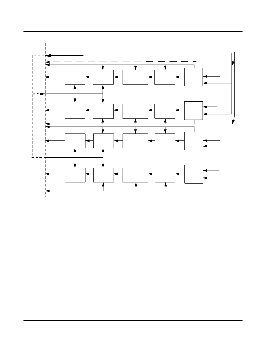
Figure 23. Receive Clocking Diagram for SONET Mode Quad-Channel Alignment in Block A – ORSO42G5
Multi-channel Alignment in SONET Mode (ORSO82G5)
The alignment FIFO allows the transfer of all data to a common clock. The FIFO sync block allows the system to be
congured to allow the frame alignment of multiple slightly varying data streams. This optional alignment ensures
that matching SERDES streams will arrive at the FPGA end in perfect data sync. It is important to note that for all
aligned channels in a group, the SERDES transmitters on the other side of the high-speed link must all be transmit-
ting data at exactly the same frequency (0 ppm difference), i.e., using a common clock source.
The ORSO82G5 has a total of eight channels (four per SERDES block). The incoming data of these channels can
be synchronized in several ways, or they can be independent of one other. Two channels within a SERDES can be
aligned together; channel A and B and/or channel C and D can form a pair as shown in Figure 24. Alternately, all
four channels in a SERDES block can be aligned together to form a communication channel with a bandwidth of 10
Gbps as shown in Figure 25.
Finally, the alignment can be extended across the SERDES blocks to align all eight channels in the ORSO82G5 as
shown in Figure 26. Individual channels within an alignment group can be disabled (i.e., powered-down) without
disrupting other channels. Note that the SERDES channel that is powered down can not be the source of the RSY-
SCLKxx that is clocking the read side of the alignment FIFO. When a disabled channel becomes active as part of
an alignment group, the group may need to be re-aligned. Then the whole group needs to be resynched. This
would only need to occur if the transmitting frame pulse for the new link is different from the rest of the group.
FPGA
RCK78A
RWCKAD
RWCKBC
RWCKBD
RWCKAC
SPE
Generator
SPE
Generator
SPE
Generator
SPE
Generator
Alignment
FIFO
Alignment
FIFO
Alignment
FIFO
Alignment
FIFO
Framer,
Descrambler
Framer,
Descrambler
Framer,
Descrambler
Framer,
Descrambler
Logic Common to Block
Common
155.52 MHz
SERDES
DEMUX
RSYSCLKA2
Channel AC
Channel AD
HDIN[P:N]_AC
2.488 Gbits/s
SERDES
HDIN[P:N]_AD
2.488 Gbits/s
DEMUX
SERDES
DEMUX
RSYSCLKB2
Channel BC
Channel BD
HDIN[P:N]_BC
2.488 Gbits/s
SERDES
HDIN[P:N]_BD
2.488 Gbits/s
DEMUX
REFCLKA[P,N]
REFCLKB[P,N]
相关PDF资料 |
PDF描述 |
|---|---|
| PIC32MX675F256L-80I/PT | IC MCU 32BIT 256KB FLASH 100TQFP |
| D38999/26FE26SC | CONN PLUG 26POS STRAIGHT W/SCKT |
| MSP430F4783IPZ | IC MCU 16BIT 48KB FLASH 100LQFP |
| MS27656T17F99S | CONN RCPT 23POS WALL MNT W/SCKT |
| VI-J4B-IW-F3 | CONVERTER MOD DC/DC 95V 100W |
相关代理商/技术参数 |
参数描述 |
|---|---|
| ORSO82G5-3FN680C1 | 功能描述:FPGA - 现场可编程门阵列 10368 LUT 372 I/O RoHS:否 制造商:Altera Corporation 系列:Cyclone V E 栅极数量: 逻辑块数量:943 内嵌式块RAM - EBR:1956 kbit 输入/输出端数量:128 最大工作频率:800 MHz 工作电源电压:1.1 V 最大工作温度:+ 70 C 安装风格:SMD/SMT 封装 / 箱体:FBGA-256 |
| ORSO82G5-G2-PAC-EV | 功能描述:可编程逻辑 IC 开发工具 ORCA ORSO82G5-FPSC Eval Brd RoHS:否 制造商:Altera Corporation 产品:Development Kits 类型:FPGA 工具用于评估:5CEFA7F3 接口类型: 工作电源电压: |
| ORSPI4 | 制造商:LATTICE 制造商全称:Lattice Semiconductor 功能描述:Dual SPI4 Interface and High-Speed SERDES FPSC |
| ORSPI4-1F1156C | 功能描述:FPGA - 现场可编程门阵列 16192 LUT RoHS:否 制造商:Altera Corporation 系列:Cyclone V E 栅极数量: 逻辑块数量:943 内嵌式块RAM - EBR:1956 kbit 输入/输出端数量:128 最大工作频率:800 MHz 工作电源电压:1.1 V 最大工作温度:+ 70 C 安装风格:SMD/SMT 封装 / 箱体:FBGA-256 |
| ORSPI4-1F1156I | 功能描述:FPGA - 现场可编程门阵列 16192 LUT RoHS:否 制造商:Altera Corporation 系列:Cyclone V E 栅极数量: 逻辑块数量:943 内嵌式块RAM - EBR:1956 kbit 输入/输出端数量:128 最大工作频率:800 MHz 工作电源电压:1.1 V 最大工作温度:+ 70 C 安装风格:SMD/SMT 封装 / 箱体:FBGA-256 |
发布紧急采购,3分钟左右您将得到回复。