- 您现在的位置:买卖IC网 > PDF目录11731 > ORT82G5-1F680I (Lattice Semiconductor Corporation)IC FPSC TRANSCEIVER 8CH 680-BGA PDF资料下载
参数资料
| 型号: | ORT82G5-1F680I |
| 厂商: | Lattice Semiconductor Corporation |
| 文件页数: | 91/119页 |
| 文件大小: | 0K |
| 描述: | IC FPSC TRANSCEIVER 8CH 680-BGA |
| 产品变化通告: | Product Discontinuation 01/Aug/2011 |
| 标准包装: | 24 |
| 系列: | * |
第1页第2页第3页第4页第5页第6页第7页第8页第9页第10页第11页第12页第13页第14页第15页第16页第17页第18页第19页第20页第21页第22页第23页第24页第25页第26页第27页第28页第29页第30页第31页第32页第33页第34页第35页第36页第37页第38页第39页第40页第41页第42页第43页第44页第45页第46页第47页第48页第49页第50页第51页第52页第53页第54页第55页第56页第57页第58页第59页第60页第61页第62页第63页第64页第65页第66页第67页第68页第69页第70页第71页第72页第73页第74页第75页第76页第77页第78页第79页第80页第81页第82页第83页第84页第85页第86页第87页第88页第89页第90页当前第91页第92页第93页第94页第95页第96页第97页第98页第99页第100页第101页第102页第103页第104页第105页第106页第107页第108页第109页第110页第111页第112页第113页第114页第115页第116页第117页第118页第119页
Lattice Semiconductor
ORCA ORT42G5 and ORT82G5 Data Sheet
73
Recommended Board-level Clocking for the ORT42G5 and ORT82G5
Option 1: Asynchronous Reference Clocks Between Rx and Tx Devices
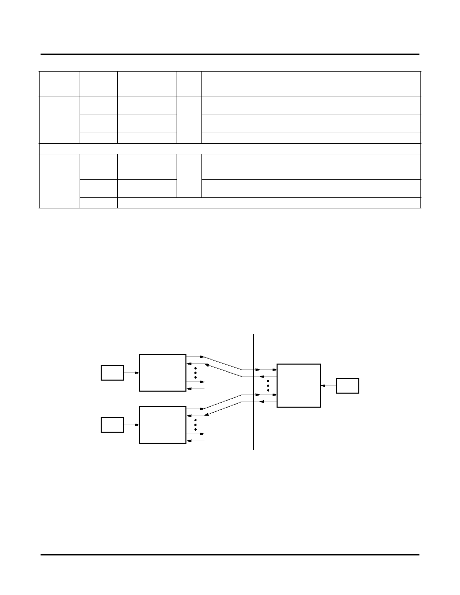
Each board that uses the ORT42G5 or ORT82G5 as a transmit or receive device will have its own local reference
clock as shown in Figure 37. Figure 37 shows the ORT82G5 device on the switch card receiving data on two of its
channels from a separate source. Data tx1 is transmitted from a tx device with refclk1 as the reference clock and
Data tx2 is transmitted from a tx device with refclk2 as the reference clock. Receive channel AA locks to the incom-
ing data tx1 and receive channel AB locks to the incoming data tx2.
The advantage of this clocking scheme is the fact that it is not necessary to distribute a reference clock (typically
156 MHz for 10GE and 155.52 MHz for OC-192 applications) across a backplane.
Figure 37. Asynchronous Clocking Between Rx and Tx Devices
Option 2: Synchronous Reference Clocks to Rx and Tx Devices
In this type of clocking, a single reference clock is distributed to all receive and transmit devices in a system
(Figure 38). This distributed clocking scheme will permit maximum exibility in the usage of transmit and receive
channels in the current silicon such as:
All transmit and receive channels can be used within any quad in receive channel alignment or alignment bypass
mode.
In channel alignment mode, each receive channel operates on its own independent clock domain.
30A02
[0:1]
RX_FIFO_MIN
00
MSb’s for the threshold for low address in RX_FIFOs. RX_FIFO_MIN, Bit
1 is MSb. Useful values for RX_FIFO_MIN [0:4] are 0 to 17(decimal).
[2]
FMPU_RESYNC8
Resynchronizes all 8 channels when it transitions from 0 to 1. Status is a
0 on device reset.
[3:7]
—
Reserved for future use.
Common Status Registers xx=[AA,...,BD]
30A03
[0]
SYNC8_OVFL
00
Read-Only Multi-Channel Overow Status. When SYNC8_OVFL=1,
8-channel synchronization FIFO overow has occurred.
SYNC8_OVFL=0 on device reset.
[1]
SYNC8_OOS
Read-Only Multi-Channel Out-Of-Sync Status. When SYNC8_OOS=1,
8-channel synchronization has failed. SYNC8_OOS=0 on device reset.
[2:7]
Reserved for future use.
Table 30. ORT82G5 Memory Map (Continued)
(0x)
Absolute
Address
Bit
Name
Reset
Value
(0x)
Description
REFCLK 1
PORT CARD #1
PORT CARD #2
TX1
TX2
BACKPLANE
AC
AD
SWITCH
CARD
REFCLK 2
REFCLK 3
ORT42G5
or
ORT82G5
ORT42G5
or
ORT82G5
ORT42G5
or
ORT82G5
相关PDF资料 |
PDF描述 |
|---|---|
| MS27474E16F35S | CONN RCPT 55POS JAM NUT W/SCKT |
| CB3106A-24-7P | CONN PLUG 16POS STRAIGHT W/PINS |
| ORT82G5-1F680C | IC FPSC TRANSCEIVER 8CH 680-BGA |
| ORT42G5-2BM484C | IC FPSC TRANSCEIVER 4CH 484-BGA |
| ORT42G5-1BM484I | IC FPSC TRANSCEIVER 4CH 484-BGA |
相关代理商/技术参数 |
参数描述 |
|---|---|
| ORT82G5-1FN680C | 功能描述:FPGA - 现场可编程门阵列 ORCA FPSC 1.5V 3.7 G b Bpln Xcvr 643K Gt RoHS:否 制造商:Altera Corporation 系列:Cyclone V E 栅极数量: 逻辑块数量:943 内嵌式块RAM - EBR:1956 kbit 输入/输出端数量:128 最大工作频率:800 MHz 工作电源电压:1.1 V 最大工作温度:+ 70 C 安装风格:SMD/SMT 封装 / 箱体:FBGA-256 |
| ORT82G5-1FN680C1 | 功能描述:FPGA - 现场可编程门阵列 10368 LUT 372 I/O RoHS:否 制造商:Altera Corporation 系列:Cyclone V E 栅极数量: 逻辑块数量:943 内嵌式块RAM - EBR:1956 kbit 输入/输出端数量:128 最大工作频率:800 MHz 工作电源电压:1.1 V 最大工作温度:+ 70 C 安装风格:SMD/SMT 封装 / 箱体:FBGA-256 |
| ORT82G5-1FN680I | 功能描述:FPGA - 现场可编程门阵列 ORCA FPSC 3.7 Gb Bp ln Xcvr 643K Gt I RoHS:否 制造商:Altera Corporation 系列:Cyclone V E 栅极数量: 逻辑块数量:943 内嵌式块RAM - EBR:1956 kbit 输入/输出端数量:128 最大工作频率:800 MHz 工作电源电压:1.1 V 最大工作温度:+ 70 C 安装风格:SMD/SMT 封装 / 箱体:FBGA-256 |
| ORT82G5-1FN680I1 | 功能描述:FPGA - 现场可编程门阵列 10368 LUT 372 I/O RoHS:否 制造商:Altera Corporation 系列:Cyclone V E 栅极数量: 逻辑块数量:943 内嵌式块RAM - EBR:1956 kbit 输入/输出端数量:128 最大工作频率:800 MHz 工作电源电压:1.1 V 最大工作温度:+ 70 C 安装风格:SMD/SMT 封装 / 箱体:FBGA-256 |
| ORT82G5-2BM680C | 功能描述:FPGA - 现场可编程门阵列 10368 LUT 372 I/O RoHS:否 制造商:Altera Corporation 系列:Cyclone V E 栅极数量: 逻辑块数量:943 内嵌式块RAM - EBR:1956 kbit 输入/输出端数量:128 最大工作频率:800 MHz 工作电源电压:1.1 V 最大工作温度:+ 70 C 安装风格:SMD/SMT 封装 / 箱体:FBGA-256 |
发布紧急采购,3分钟左右您将得到回复。