- 您现在的位置:买卖IC网 > PDF目录12023 > P89V51RD2FN,112 (NXP Semiconductors)IC 80C51 MCU FLASH 64K 40-DIP PDF资料下载
参数资料
| 型号: | P89V51RD2FN,112 |
| 厂商: | NXP Semiconductors |
| 文件页数: | 60/80页 |
| 文件大小: | 0K |
| 描述: | IC 80C51 MCU FLASH 64K 40-DIP |
| 产品培训模块: | Migrating from 8/16-Bit MCUs to 32-Bit ARMs |
| 标准包装: | 9 |
| 系列: | 89V |
| 核心处理器: | 8051 |
| 芯体尺寸: | 8-位 |
| 速度: | 40MHz |
| 连通性: | SPI,UART/USART |
| 外围设备: | 欠压检测/复位,POR,PWM,WDT |
| 输入/输出数: | 32 |
| 程序存储器容量: | 64KB(64K x 8) |
| 程序存储器类型: | 闪存 |
| RAM 容量: | 1K x 8 |
| 电压 - 电源 (Vcc/Vdd): | 4.5 V ~ 5.5 V |
| 振荡器型: | 内部 |
| 工作温度: | -40°C ~ 85°C |
| 封装/外壳: | 40-DIP(0.600",15.24mm) |
| 包装: | 管件 |
| 产品目录页面: | 706 (CN2011-ZH PDF) |
| 配用: | 622-1017-ND - BOARD 44-ZIF PLCC SOCKET 622-1001-ND - USB IN-CIRCUIT PROG 80C51ISP |
| 其它名称: | 568-2431-5 935277948112 P89V51RD2FN |
第1页第2页第3页第4页第5页第6页第7页第8页第9页第10页第11页第12页第13页第14页第15页第16页第17页第18页第19页第20页第21页第22页第23页第24页第25页第26页第27页第28页第29页第30页第31页第32页第33页第34页第35页第36页第37页第38页第39页第40页第41页第42页第43页第44页第45页第46页第47页第48页第49页第50页第51页第52页第53页第54页第55页第56页第57页第58页第59页当前第60页第61页第62页第63页第64页第65页第66页第67页第68页第69页第70页第71页第72页第73页第74页第75页第76页第77页第78页第79页第80页
2009-2011 Microchip Technology Inc.
DS39960D-page 63
PIC18F87K22 FAMILY
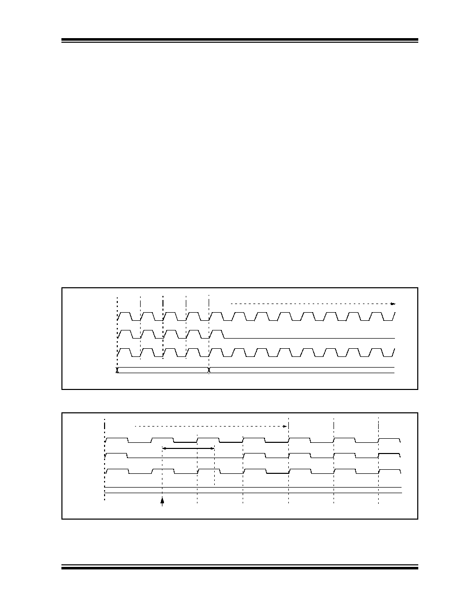
4.4.1
PRI_IDLE MODE
This mode is unique among the three low-power Idle
modes, in that it does not disable the primary device
clock. For timing-sensitive applications, this allows for
the fastest resumption of device operation with its more
accurate, primary clock source, since the clock source
does not have to “warm-up” or transition from another
oscillator.
PRI_IDLE mode is entered from PRI_RUN mode by
setting the IDLEN bit and executing a SLEEP instruc-
tion. If the device is in another Run mode, set IDLEN
first, then clear the SCS bits and execute SLEEP.
Although the CPU is disabled, the peripherals continue
to be clocked from the primary clock source specified
by the FOSC<3:0> Configuration bits. The OSTS bit
remains set (see Figure 4-7).
When a wake event occurs, the CPU is clocked from the
primary clock source. A delay of interval, TCSD
(Parameter 39, Table 31-13), is required between the
wake event and the start of code execution. This is
required to allow the CPU to become ready to execute
instructions. After the wake-up, the OSTS bit remains
set. The IDLEN and SCS bits are not affected by the
wake-up (see Figure 4-8).
4.4.2
SEC_IDLE MODE
In SEC_IDLE mode, the CPU is disabled but the
peripherals continue to be clocked from the SOSC
oscillator. This mode is entered from SEC_RUN by set-
ting the IDLEN bit and executing a SLEEP instruction. If
the device is in another Run mode, set the IDLEN bit
first, then set the SCS<1:0> bits to ‘01’ and execute
SLEEP
. When the clock source is switched to the SOSC
oscillator, the primary oscillator is shut down, the OSTS
bit is cleared and the SOSCRUN bit is set.
When a wake event occurs, the peripherals continue to
be clocked from the SOSC oscillator. After an interval
of TCSD following the wake event, the CPU begins
executing code being clocked by the SOSC oscillator.
The IDLEN and SCS bits are not affected by the wake-
up and the SOSC oscillator continues to run (see
FIGURE 4-7:
TRANSITION TIMING FOR ENTRY TO IDLE MODE
FIGURE 4-8:
TRANSITION TIMING FOR WAKE FROM IDLE TO RUN MODE
Q1
Peripheral
Program
PC
PC + 2
OSC1
Q3
Q4
Q1
CPU Clock
Clock
Counter
Q2
OSC1
Peripheral
Program
PC
CPU Clock
Q1
Q3
Q4
Clock
Counter
Q2
Wake Event
TCSD
相关PDF资料 |
PDF描述 |
|---|---|
| P89V51RC2FN,112 | IC 80C51 MCU FLASH 32K 40-DIP |
| P89V51RC2FBC,557 | IC 80C51 MCU FLASH 32K 44-TQFP |
| 292303-1 | CONN USB RECEPT R/A TYPE A 4POS |
| VI-B3V-CU-B1 | CONVERTER MOD DC/DC 5.8V 200W |
| VJ1825A562KBCAT4X | CAP CER 5600PF 200V 10% NP0 1825 |
相关代理商/技术参数 |
参数描述 |
|---|---|
| P89V52X2 | 制造商:PHILIPS 制造商全称:NXP Semiconductors 功能描述:8-bit 80C51 low power 8 kB flash microcontroller with 256 B RAM, 192 B data EEPROM |
| P89V52X2FA | 制造商:PHILIPS 制造商全称:NXP Semiconductors 功能描述:8-bit 80C51 low power 8 kB flash microcontroller with 256 B RAM, 192 B data EEPROM |
| P89V52X2FA,512 | 功能描述:8位微控制器 -MCU 80C51 8K FL / 256 RM RoHS:否 制造商:Silicon Labs 核心:8051 处理器系列:C8051F39x 数据总线宽度:8 bit 最大时钟频率:50 MHz 程序存储器大小:16 KB 数据 RAM 大小:1 KB 片上 ADC:Yes 工作电源电压:1.8 V to 3.6 V 工作温度范围:- 40 C to + 105 C 封装 / 箱体:QFN-20 安装风格:SMD/SMT |
| P89V52X2FBD | 制造商:PHILIPS 制造商全称:NXP Semiconductors 功能描述:8-bit 80C51 low power 8 kB flash microcontroller with 256 B RAM, 192 B data EEPROM |
| P89V52X2FBD,157 | 功能描述:8位微控制器 -MCU 80C51 8K FL / 256 RM RoHS:否 制造商:Silicon Labs 核心:8051 处理器系列:C8051F39x 数据总线宽度:8 bit 最大时钟频率:50 MHz 程序存储器大小:16 KB 数据 RAM 大小:1 KB 片上 ADC:Yes 工作电源电压:1.8 V to 3.6 V 工作温度范围:- 40 C to + 105 C 封装 / 箱体:QFN-20 安装风格:SMD/SMT |
发布紧急采购,3分钟左右您将得到回复。